This thread has been locked.

If you have a related question, please click the "Ask a related question" button in the top right corner. The newly created question will be automatically linked to this question.

ADS1198: Range for single-ended or differential use

Part Number: ADS1198
Other Parts Discussed in Thread: ADS1299

Good day,

I would like to use the ADS1198 in a unipolar configuration for a signal that can range between 0 and 5V. To do this I plan to tie all INN at 2.5 and have my input signals on INP and configure the registers for vref = 4V. However while reading the datasheet I am getting the impression of reading two differing pieces of information :

"The analog input to the ADS1198 is fully differential. Assuming PGA = 1, the differential input (INP – INN) can span between –VREF to +VREF."

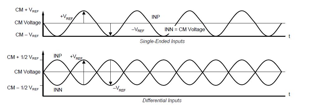
"When the input is single-ended, the INN input is held at the common-mode voltage, preferably at mid-supply. The INP input swings around the same common voltage and the peak-to-peak amplitude is the (common-mode + 1/2VREF) and the (common-mode – 1/2VREF)."

If I believe the later version I would only be able to mesure tensions from 0.5V to 4.5V for a common mode of 2.5V. Am I understanding this correctly ? If so how can I use this device for the above specified need ?

  • Hi Cailyn,

    Welcome to our forum and thanks for your post!

    You have found a typo in our datasheet. Figures 17 and 18 should show a sine wave with amplitude equal to VREF:

    On a unipolar 5-V supply and with INN = 2.5 V, the maximum differential input swing can be -2.5 V to + 2.5 V, assuming Gain = 1. This would indicate that the signal on INP is swinging from 0 V to 5 V and centered around the same 2.5 V common-mode.

    Remember that the differential input voltage to the PGA must always remain less than VREF / Gain. For example, with VREF = 4 V and Gain = 8, your input signal on INP can range from Vcm - 500 mV to Vcm + 500 mV (i.e. INP = 2 V to 3 V, INN = Vcm = 2.5 V).

    Best Regards,

  • Hello,

    Thank you for this answer, while it does answer my original question, I now have another one. While searching for another component that may be a solution to the problem, I came across the ADS1299, which is very similar. The datasheet contains these pieces of information :

    "The outputs of the amplifiers in Figure 23 cannot swing closer to the supplies (AVSS and AVDD) than 200 mV. If

    the outputs of the amplifiers are driven to within 200 mV of the supply rails, then the amplifiers saturate and

    consequently become nonlinear"

    and :

    In the datasheet of the ADS1198 I found the same formula but not the same explanation as above regarding the 200 mV, is this information also accurate for the original component ? This would therefore mean I could not surpass 0.2 and 4.8V for AVDD = 5V and AVSS = 0V if I understand correctly.

  • Hi Cailyn,

    The description applies to both devices, it's just that the ADS1299 datasheet was updated more recently to provide more clarity.

    The 200 mV headroom is the output limitation of each amplifier used in the ADS1x9x PGA for linear operation. The absolute voltage at each amplifier output may not be able to range all the way to the supply rails, but you can still achieve a differential output voltage that equals the ADC full-scale  (= +VREF or -VREF). The common-mode voltage should be set close to mid-supply in order to give each amplifier equal swing above or below the common-mode.

    Best Regards,

  • Hello Ryan,

    Thank you for your time !

    Cailyn