This thread has been locked.

If you have a related question, please click the "Ask a related question" button in the top right corner. The newly created question will be automatically linked to this question.

DAC8718: Unexpected POR behavior for outputs

Part Number: DAC8718

I have included the schematics for the DAC subcircuit and the power sequecers as a .docx.  Hopefully they are readable. 

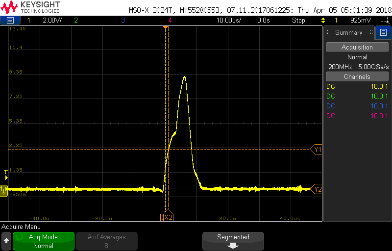
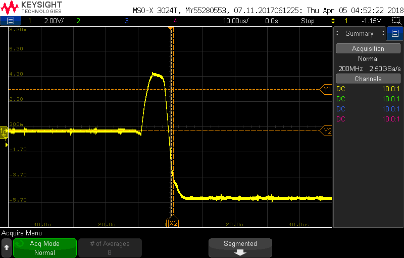
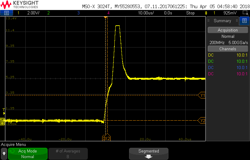
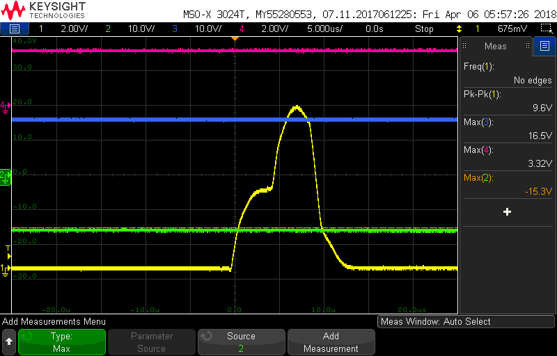
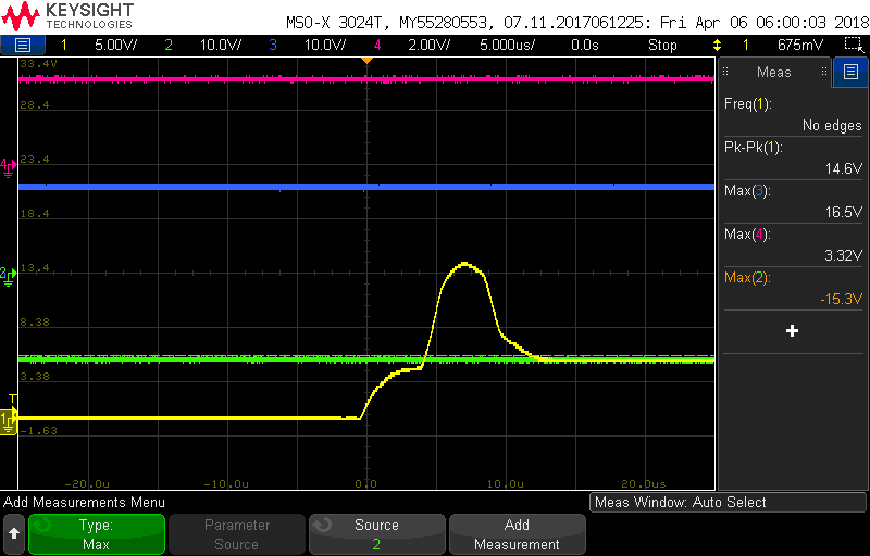
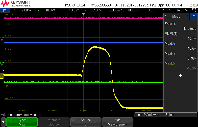
Now to the issue.  We are running the DAC8718 in bipolar mode (+/-16.5V) and we have RSTSEL set to IOVdd and #USB tied to GND.  With a 4.096V reference on REFA and B (and it is truly a reference that is not tied to any other parts) we see 12.288V on the DAC outputs on boot.  If we ground CLR, it will pull the outputs to 0V, but a RST or LDAC cycle will return them to 12.288V.  If we boot the device and read the offset registers, they are 0x0000.  If we write to 0x999A to them, the voltage on the outputs go to 0V and we can read the same value out of the registers that we wrote in (this seems to indicate the chip believes we are in bipolar mode as well.)

Why isn't the output of the chip on bootup behaving as datasheet seems to state it should (0x999A being loaded automatically).  This is problematic as our down stream devices cannot tolerate the 12+V supply.

Our power supplies are being sequenced explicitly by the LM3880MF-1AA chips as well.  with 3V3(2) on flag-A1 (IOVdd), 5V(2) on flag-A2 (DVdd), 16V5 on flag-A3 (AVdd), -16V5 on flag-A4 (AVss) and our reference on flag-A5 (REF).

I have connected an EVM to bench supplies where IOVdd=DVdd=5V on a power supply, AVdd = 16.5V on a power supply, AVss = -16.5V on a power supply and using the onboard 5V reference with the sequence of 5V -> 16.5V -> -16.5V being turned on and it has the same behavior.

Any suggestions?

DAC-TI.docx

  • Hi Adam,

    Welcome to E2E and thank you for your query. I will check the test conditions on the EVM and get back with my findings by end of this week.

    Hope that is fine with you.

    Regards,
    Uttam Sahu
    Applications Engineer, Precision DACs
  • Hi Adam,

    I somehow couldn't find time to check your test case. I will try to finish it by coming Tuesday. My apologies for the delay.

    Regards,
    Uttam
  • Uttam,

    Thanks for the update.  I have been working in parallel on more of a brute force solution.  My idea was to hold the #CLR low, set up the registers that are incorrect by hand (OFFSET_A and B), release the CLR and send a latch command, hoping to avoid any glitches on the Vouts.

    If I do the above procedure, I see a ~5us 4.5V(ish) glitch on the Vouts when I issue the LD command (REG_WRITE to CFG with A/B and LD bits high).  Interestingly, this glitch manifests each time I issue the LD command, even in rapid fire, which confuses me completely.  It is almost as if the +leg of the opamp is fed before the latch command and the -leg gets voltage at the latch command.  All in all, much better overall (not coming to 12+V), but it still has the ability to compromise my down stream devices.

    I then spent a bit of time looking a the datasheet and saw that handy little switch on the right edge of the functional block diagram on page 10 (with a strikingly similar pic on page 40).  If the drawing is accurate to the circuit, it looked like I could write a 1 to both the PD bits in the config register, do all my register massaging, throw the LD pin (writing 1 to the PD's as well) wait a ms to stabilize internally and THEN clear the PD bits.  

    In practice, this has the same output glitching that I was encountering with just using the LD command without powering down the groups ahead of time.  So my assumption is that this switch is implemented differently than represented in the diagrams (i.e. NOT on the output of the OpAmp with nothing else between it and the output pin.)

    That is where I am at the moment.  I am still very interested in getting the POR response to be accurate to datasheet, but I am trying to hammer this circuit into shape with the controls I have available (with limited success).

    Adam

  • Hi Adam,

    My apologies for the delay in replying. I tested this on the EVM and saw that a similar behavior happens when there is a problem with the power supply sequencing. I couldn't get any power sequencing information from your schematics. Please refer page# 44 in datasheet and check whether you are following that or not. I think this should resolve your issue.

    Please let me know if the issue still persists after the above fix.

    Regards,
    Uttam
  • Uttam,

    Sorry for the late reply, I was busy with other fires...  The initial document I posted has the sequencers for the DAC rails on the second page and the outputs of these sequencing flags goes to the enables on the particular regulators.  I told you our voltage sequencing in the original post, but I will paste it here as well.

    "Our power supplies are being sequenced explicitly by the LM3880MF-1AA chips as well.  with 3V3(2) on flag-A1 (IOVdd), 5V(2) on flag-A2 (DVdd), 16V5 on flag-A3 (AVdd), -16V5 on flag-A4 (AVss) and our reference on flag-A5 (REF)."

    I also told you the set up for the EVM I was using as well for sequencing.

    "I have connected an EVM to bench supplies where IOVdd=DVdd=5V on a power supply, AVdd = 16.5V on a power supply, AVss = -16.5V on a power supply and using the onboard 5V reference with the sequence of 5V -> 16.5V -> -16.5V being turned on and it has the same behavior."

    The EVM sequencing was done by a human turning on the supplies by hand, so there is no tight timings on that.

    As far as I can tell, I am following the prescribed sequencing on P44.

    Adam

  • Adam,

    I did the same power sequencing on EVM as you mentioned and I didn't see any issue. Only when I switched on the 5V to MMB0 after the +/-16.5V was on, did I notice the problem you described.

    I think we might be missing something. Just to make an apple-to-apple comparison, let's use the EVM for debugging. Could you please measure the VREFA, VREFB, OFFSETA and OFFSETB on EVM at the following conditions:

    1. MMB0 5V supply turned on after +/-16.5V supply
    2. MMB0 5V supply turned on before +/-16.5V supply

    Regards,
    Uttam
  • Uttam,

    We found a significant issue with the rail bring up on our board. Our 5V (Dvdd) is limited to 60mA (by an iLIM) and 150mA by chip.  When we bring up our -16V5 rail, we see our 5V dragged down to a negative voltage for about 10mS as the AVss rail comes up.  When the 5V rail bottoms out, something releases inside the DAC and the 5V rail rebounds.  The DAC chip is the ONLY place that either the 5V and -16V5 rails service (neither rail goes anywhere else on the board.)

    This explains the "bad sequencing" results even though both rails were up in the correct order initially, the -16V5 blinks the DVdd rail and it then comes up AFTER AVss. 

    Once we found this behavior, I removed the 5V rail from the system (removed the output inductor) and pushed this rail in with a bench supply.  If we choke the supply to 5V@300mA, we find that the bench supply will maintain 5V, but the current coming out of the 5V rail is 180mA for almost 450mS.  If we choke the supply to 5V@150mA, OCP kicks in on the bench supply, the rail sags to about 2.5V@150mA for 500mS.  The last test we set the current limit on the supply to 60mA (to mimic board), when the -16V5 rail started coming up, the 5V supply collapsed to ground in about 50mS, the current draw goes away and the rail rebounds to 5V quickly.

    We suspect that there is some interaction between the 2 rails inside the DAC as these 2 rails ONLY go to our DACs (3).  Since we are using the QFN part, we had limited ability for pin lift, so we cut our 5V traces (Pins 17 and 42) to one of our 3 DACs on the board (all connected to same supplies and based on the same exact template in Altium.)  When we did this, the current consumed was 120mA on the 5V rail during the -16V5 come up, 2/3 of the 3 DACs connected current.  So it appears that we are seeing the same behavior across all 3 DACs evenly.

    I have scrubbed both the schematic and layout of the parts and can see nothing that violates datasheet.  Our biggest suspicion is that the exposed pad being tied to AVss is the source of our woes somehow.  It is a little unsettling the guidance that is given about this pad in the footnote on P11:

    "The thermal pad is internally connected to the substrate. This pad can be connected to AVSS or left floating. Keep the thermal pad separate from the digital ground, if possible."

    I am having our tech populate one of the DACs with kapton covering the pad so we can test this theory.  Other than that, I am at somewhat of a loss as to what is going on.  We know it is an interaction inside the 8718 between these 2 rails (based on our isolation testing), but we are running out of possible problems.

    Thanks for helping us,

    Adam

  • Uttam,

    I ran the tests on the EVM after we found the problem I described below and found that there was no such interaction between DVdd and AVss on the EMV as we saw on our board. We ran the test first from bench supplies and then we powered the EVM off of our generated rails as well with no bad interactions.

    Because we are using the QFN package, the most significant difference between the EVM and our solution is the thermal pad, so we are trying to disconnect the pad in our design for testing. The problem is that our layout guy is good and REALLY connected that pad to AVss... ;)

    Adam
  • Adam,

    Glad to know that you are able to have some progress on the debugging. Let's see if the AVSS tied to thermal pad is the culprit, in which case I will take the feedback to update the datasheet.

    Another doubt - I am not sre whether you have already mentioned this or not, but you are seeing the behavior across boards, right? Please make sure this is not specific to one board only.

    In the meanwhile, is it possible to share a snapshot of the layout around the DAC? I will try to see if there can be other mechanisms that might be playing a role here.

    Regards,
    Uttam
  • Attached is the layout view.  First pic is a snip with all layers.  Second is with just top and silk.  Third is Top isolated.  Fourth is the chip zoomed in for pins and orientation.

    Adam

    TI-Layout.docx

  • Thanks, Adam for the layout information. I will analyze and get back by Monday on this.

    Regards,
    Uttam
  • Hi Adam,

    I got some hint from the design team that this device requires higher current on the DVDD pin during startup. You can try that in your test. I couldn't get an exact number for the current though.

    Please let me know if that helps.

    Regards,
    Uttam
  • Hi Adam,

    Did you get a chance to test with higher current limit on DVDD? Please let me know if you have some findings?

    Regards,
    Uttam
  • We have.  We have 3 DACs hooked up to our rails and we found that DVdd pulls about 60mA per DAC for about 350mS precisely when the AVss rail is being brought up.


    Adam

  • We have reorganized our circuit some so that the 5V(2) rail has been eliminated (we were using it for DVdd but it was sized per datasheet requirements and not the undocumented higher current at startup so it was collapsing.)  We ended up depopping the 5V rail and using our 3V3(2) rail to supply both IOVdd and DVdd together.  In order to do this, we had to change our references (originally 4.096V to 1.8V) to be under the new DVdd.  Now that we can start the chip without driving our DVdd rail into OCP, we are seeing some strange behavior on the initial latch of our rails.

    Because we are seeing the chip come up with incorrect offsets, we are manually setting  our registers for operation.

    The code looks like:

    bool DAC8718_Initialize()

    {    

       DAC8718_RegisterLoad(ALL_DACS, DAC_Write, DAC_Addr_CONFIG_REG, DAC_Data_CONFIG_REG_DEFAULT);

       DAC8718_RegisterLoad(ALL_DACS, DAC_Write, DAC_Addr_OFFSET_A, DEFAULT_6_OFFSETDAC_CODE);

       DAC8718_RegisterLoad(ALL_DACS, DAC_Write, DAC_Addr_OFFSET_B, DEFAULT_6_OFFSETDAC_CODE);

       DAC8718_RegisterLoad(ALL_DACS, DAC_Write, DAC_Addr_DAC_BROADCAST, 0x8000);

       DAC8718_RegisterLoad(ALL_DACS, DAC_Write, DAC_Addr_CONFIG_REG, DAC_Data_CONFIG_REG_DEFAULT | 0x4000);

       return true;

    }

    we do some checking in the middle to make sure values stuck, but I have removed it for clarity.  Essentially, we set everything up to be 0V and then latch the values forward.

    If I run this code, this I was I get on the DAC output pins:

    Why does this run up to 9V before going to the 0V it is supposed to be?  Why does this exceed the 3xVref (in our case 5.4V) ever?

    If I drive it to the floor on initialize by changing the broadcast line:

       DAC8718_RegisterLoad(ALL_DACS, DAC_Write, DAC_Addr_DAC_BROADCAST, 0x0000);

    I see this on the DAC output pins:

    Why does it go positive to go low?

    If I change the broadcast line to drive the DAC high at boot:

       DAC8718_RegisterLoad(ALL_DACS, DAC_Write, DAC_Addr_DAC_BROADCAST, 0xFFFF);

    I see this:

    It is artificially clipped, but why the overshoot?

    All in all, this DAC is not behaving well...

    Adam

  • Adam,

    This looks like some power integrity issue. We usually don't see this large code-to-code glitch. Could you also plot the power supplies during this transition?

    Regards,
    Uttam
  • So here are the 3 grabs.  In each, yellow (bottom trace) is the output of the DAC for each case.  Red(ish) is the 3V3 rail, which is IOVdd and DVdd.  Blue is the 16V5 (AVdd) and green is the -16V5 rail (AVss).  They are shown with their grounds in the same place for convenience.  

    The first trace is for when we set the output to be 0V (0x8000):

    There seems to be no distress on the rails here even though the glitch is large.

    Next is the code for going to max rail.  Our references are 1.8V now, so this should be ~5.4V (I had to shrink the range to 5V/div to get the whole overshoot):

    Again, nothing seems wrong with the supply rails.

    Lastly we have setting it to the floor (0x0000) which should be -5.4V:

    Again, the rails look pretty solid even though we have this glitch that runs up before it goes down to intended output voltage.

    Adam

  • Adam,

    Let me check this with the team and get back. What is the output load, by the way. can you try putting an RC load and see if this reduces. You can use something like 5K || 200pF

    Regards,
    Uttam
  • Here are the results with 5.1k//220pF as a load/decoupler.

    With the load:

    without the load:

    I see the work of the 220pF, but not the effect of the load in general wrt straightening out the response.


    Adam

  • Hi Adam,

    The glitches you are observing are very unrealistic as far as the DAC is concerned. I am not very sure what could be causing this. The DAC8718 being an old part, the last thing I would do is to doubt the device. Could you please find out if there is any coupling between the outputs and power supplies? You can also check the same conditions on EVM and other boards.

    Regards,
    Uttam
  • Uttam,

    Thank you for your efforts.  We will make the DAC as circuit safe as possible given the current state of outputs and replace it with a different part when we spin the board. 

    Hopefully the new part will behave more realistically!

    Adam