


Part Number: DAC38RF82EVM
Other Parts Discussed in Thread: DAC38RF82, ADC12J4000EVM
Hi Everyone,
I'm trying to interface DAC38RF82EVM with a FPGA board. I already finished a project which uses single (8bits) DAC with a sampling rate of 9GSPS.
Now I want to configure the DAC to operate in dual (12bits) DAC mode. I checked the datasheet of DAC38RF82 and found a table as follows:
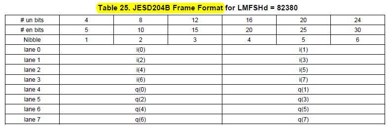
In my understanding, the i corresponds to DAC A and q corresponds to DAC B, and each of them has 12bits.
However, the JESD204B core in Vivado only accepts 32bits input in each JESD lane which is not divisable by 12. Can anyone tell how to arrange the data in JESD frame?
I also noticed that the JESD serial lane rate is 11250MHz if I set the DAC to operate in 3GPS, dual channel mode and 12bits resolution. Does this mean the JESD core clock is 11250MHz/40 = 281.25MHz? If this is true, each DAC will receive 3000/281.25 = 10.6667 samples during a FPGA clock cycle, which is not an integer. Is there anything wrong in my understanding?
Thank you.
