Because of the Thanksgiving holiday in the U.S., TI E2E™ design support forum responses may be delayed from November 25 through December 2. Thank you for your patience.

This thread has been locked.

If you have a related question, please click the "Ask a related question" button in the top right corner. The newly created question will be automatically linked to this question.

ADS8568: AD8658 power and interface

Part Number: ADS8568

Dear TI,

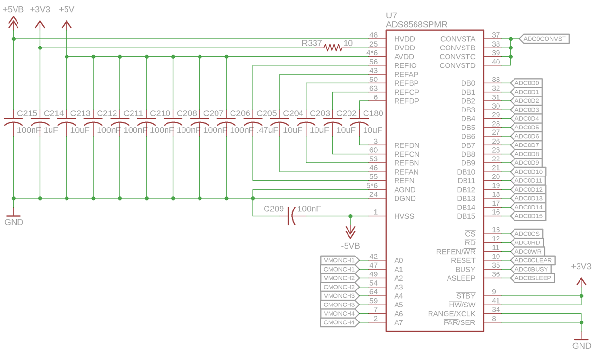
I have attempted to design a circuit for the ADS8568 and would appreciate a review and design guidance.

My design goal for this is to use the parallel interface to a microcontroller and sample from 8 channels simultaneously at maximum speed. Input signals are in the range 0-3.3V centered at 1.65V.

My main worries:

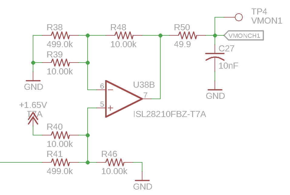
  1. On each analog input, I have this circuit which only has 49.9 ohms of resistance and a 10nF capacitor. I will probably replace the 10nF capacitor with 4.7nF to get the -3dB frequency above the sampling rate, but would appreciate any recommendations. My understanding is that this amplifier must be powered after the ADC. Should I add an extra resistor to limit current into the ADS8568? Is the extra input filtering capacitor unhelpful due to the internal capacitance?
  2. What power sequencing is required? Right now my ±5VB supplies become active two seconds after AVDD and DVDD, is this okay?
  3. Can I operate this device with ±4-VREF and a 2.5V reference from this ±5V HVDD/HVSS supply or do I need more overhead?
  4. My read is that the RESET line needs to be held low in normal operation. This is flipped from most RESET lines so I wanted to confirm before hardwiring.
  5. Should I instead use a choke on DVDD rather than a 10 ohm resistor?
  6. Should there be a 10uF capacitor in addition to the 100nF capacitor for HVDD and HVSS?
  7. I am going to use the PM version without the pad underneath. Are there recommended ground plane connections in this situation? Should I avoid running any traces under the chip and leave that as a continuous ground plane?

  • 1. The op amp must be able to drive the capactive load and settle within the aquisition time, plus the internal capacitance (10pF using higher range), if so then you are fine. There is good material on this on TIPL-ADCs section 5 that provide background as to how to refine the driving circuitry. The op amp can be powered on after the ADC, but do you mind me asking where you read that? If the op amp is being powered by HVDD and HVSS, then it is recommended that AVDD be pulled up before HVDD/HVSS.

    2. Generally, there are no specific requirements with regard to the power sequencing of the device. However, when HVDD is supplied before AVDD, the internal electrostatic discharge (ESD) structure conducts, increasing the IHVDD beyond the specified value until AVDD is applied, thus you are fine.

    3. You need more head room, HVDD and HVSS need to be higher (or lower) than your expected manx and min analog input signals. HVSS and HVDD drive the analog input circuitry, you can experience degradation in performance if not.

    4. Your understanding is correct.

    5. With proper decoupling capacitors, it should not be neccesary to add more to the DVDD line, if your application does not use any isolation. Be sure to follow good layout practices.

    6. Yes, proper decoupling in neccesary to ensure performance.

    7. There is no need to add an extra ground plane under the device is the pad is not present. You can place traces beneath the device if necessary. The datasheet, page 47 shows an example of how to route the input channels. Make sure to connect the ground pins directly to ground, and properly prioritze capactiors.

    Regards

    Cynthia

    Generally, there are no specific requirements with regard to the power sequencing of the device. However, when

    HVDD is supplied before AVDD, the internal electrostatic discharge (ESD) structure conducts, increasing the

    IHVDD beyond the specified value until AVDD is applied.

  • Thank you Cynthia! The reason for my confusion on the power sequencing is from reading some other articles here first before I posted my questions.

    This one: e2e.ti.com/.../2165816

    According to the reply:
    "2. Analog input voltage should be available later than HVDD/HVSS or at the same time, because Analog input voltage is limited between HVSS-0.3~HVDD+0.3V according to Absolute maximum Ratings table in datasheet."

    In my case, that preamp ISL28210 is powered before the HVDD/HVSS power supply being active and will be outputting a value from 0-3.3V immediately. I actually have 12 supplies on my board. The ISL28210 is powered by a ±15V supply. However, the ±15V supply powers the +5VB and -5VB supplies, so the opamps will be active before the HVDD/HVSS is powered. Worse, the +15V supply comes on 2 seconds before the -15V supply (so +HVDD and -HVDD come on at different times).

  • That is a concern.
    Since you will need to increase HVDD/HVSS, could you power those rails from the same +/- 15V that the op amps will be powered of off. This would fix the original issue of needing more head room on HVSS/HVDD and fix the concern about having an analog input signal before the rails are up.
    It is not a concern that the positive rail comes up before the negative rail for the ADC. If you do change HVSS/HVDD to the same +/-15 rails, and, I am assuming that the op amp will not be able to output anything beyond the rails available to it, then this shouldn't be an issue either with the analog input to the ADC.
    Regards
    Cynthia
  • Great, thank you for the guidance.