


Part Number: ADC12DJ3200
Other Parts Discussed in Thread: LMK04828
- Conditions
One XC7VX690T carries two ADC12DJ3200 FPGA Mezzanine Cards. The structure of FMC is as follows.
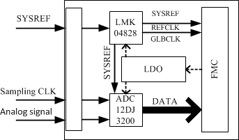
The LMK04828 is configured in 0-delay mode and provides SYSREF, REFCLK, GLBCLK.
The LMK04828 is first configured through SPI, then the ADCs are configured through SPI.
The ADCs use JMODE0.
- Phenomenon
When using the JESD204B Test Pattern Control Register (address = 0x205) = 4: Ramp test mode, the two ADCs acquire synchronization, that is, data from two ADCs can be aligned every time power on (draw waveforms in matlab).
Other conditions remain the same. When only change the JESD204B Test Pattern Control Register (address = 0x205) to 0: Normal operation, the Analog signal is supplied with a sine wave divided by a power divider from a signal source. Draw waveforms in matlab. Under one configuration conditions, the relative relationship of the starting point will not change with each trigger. But not aligned. By reconfiguring the ADC via SPI, the starting position of the acquired data will change.
- Questions
1, In the Ramp test mode, the two ADCs are synchronized, and in the normal operation mode the acquired data is not aligned. This indicates that the JESD204B link synchronization and ADC core acquisition are not synchronized. Is this correct?
2, Is there any special timing for ADC initialization when two ADCs are synchronized? For example reset the ADC cores.
3, Are there special requirements with SPI clock?
4, What else can be done?
Thank you in advance for your answers.

