This thread has been locked.

If you have a related question, please click the "Ask a related question" button in the top right corner. The newly created question will be automatically linked to this question.

CCS/ADS124S06: Please help me to debug about ads124s06 at arduino board

Part Number: ADS124S06

Tool/software: Code Composer Studio

Hi everyone,

I have question about ads124s06 controlled. I can command and r/w ads124s06 register. However, it can't work when I command it to start convert. 

The code and connect pin are at the last.

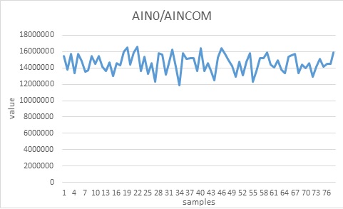
Its DRDY pin doesn't  fall at default setting. After I enable the PGA gain setting 1, I received  7FFFFFh at AIN2/AINCOM (about 2.65 volt) or 800000h at AIN0/AIN1 (about 0.02 volt). It is the max/minimum number for the ADC. It is strange.

Could anyone help me to fix this problem?

Thanks.

CONNECT PIN

PIN function connect
1 AINCOM 0
2 AIN5 2.12
3 AIN4 2.63
4 AIN3 2.05
5 AIN2 2.65
6 AIN1 2.23
7 AIN0 2.21
8 START pin11
9 CS pin53
10 DIN pin51
11 SCLK pin52
12 DOUT pin50
13 DRDY pin12
14 DGND 0V
15 IOVDD 5V
16 DVDD 3.3V
17 CLK 0
18 RESET pin13
19 GPIO3 NA
20 GPIO2 NA
21 GPIO1 NA
22 GPIO0 NA
23 REFOUT 1uF to AVSS
24 REFCOM 0
25 NC NA
26 AVDD 5
27 AVSS 0
28 AVSS-SW 0
29 REFN0 2.5
30 REFP0 0
31 REFN1 2.5
32 REFP1 0

Arduino CODE

#include <SPI.h>
#include <TimerOne.h>
#define START 11
#define DRDY 12
#define RESET 13
const int CS = 53;
int stat;
int stat1;
int stat2;
int stat3;
int stat4;
int stat5;
volatile int DRDY_state = LOW;
SPISettings settings1(4000000, MSBFIRST, SPI_MODE1); 
void setup() {
SPI.begin();
pinMode(CS,OUTPUT);
pinMode(RESET, OUTPUT);
pinMode(DRDY, INPUT);
pinMode(START,OUTPUT);
digitalWrite(RESET , HIGH); 
Serial.begin(115200);
SPI.beginTransaction(settings1);
digitalWrite(CS, LOW);
digitalWrite(STA,LOW);
}
void loop() {
for(int i=0;i>=0;i++)
if(i==0){
SPI.transfer(0x42); // WREG register adress
SPI.transfer(0x02); // WREG byte number -1
SPI.transfer(0x1C); // WREG write AIN2-AINCOM
SPI.transfer(0x00); // 03h PGA reg(00h to closed, 08h to Gain=1 )
SPI.transfer(0x10); // DATA RATE 2.5 SPS
SPI.transfer(0x08); // start converting command
delayMicroseconds(10);
}
else
{
//Serial.println("start converting");
SPI.transfer(0x12); //RDATA command
delayMicroseconds(10);
stat = SPI.transfer(0) ; // get data from miso
stat1= SPI.transfer(0);
stat2= SPI.transfer(0);
Serial.println("ADC output");
Serial.println(stat);
Serial.println(stat1);
Serial.println(stat2);
}
SPI.endTransaction();
}
  • Hi user5046138,

    Welcome to the E2E forum! The are a few items to consider.  First let's take a look at the code.  In the Setup block you have defined START but when writing to the pin you use STA as an abbreviation.  Make sure the START pin is not floating.  In the Loop block, you use a for() function without {}.  You also set the data rate to 2.5sps, but only wait 10us before attempting to read.  See Table 13 on page 42 of the ADS124S06 datasheet for actual time for conversion to end which for your configuration will be 406.504ms.  Also your configuration is using AIN1/AINCOM (0x1C) as opposed to AIN2/AINCOM (0x2C).  So you must make sure START is not floating and the configuration is as you would expect, and make sure you wait the minimum time before checking for DRDY to go low.

    As far as the IC connections, the reference inputs are connected in reverse.  REFP should be the most positive value and REFN the most negative, so you have the pin connections reversed.

    Make sure that you are also interpreting the results properly. 0x7FFFFF is positive full-scale and 0x800000 is negative full-scale.  Most likely values will be incorrect even if the conversion has completed as the reference inputs are incorrect.

    For checking DRDY, you should check prior to attempting to read from the ADS124S06 as DRDY will be forced high when the device is read (SCLK forces DRDY high) and you are attempting to read almost continuously in your code.

    Best regards,

    Bob B

  • Hi Bob,

    Thank you for your response. I am modifying it according to your suggestion.  I make REFP to 5 Volt and REFN to 0 Volt.  But I have another problem now. I select AIN0/AINCOM (2.21 Volt) it convert value 15514490( ECBB7A h, averaged). However, AIN1/AIN0(0.02 Volt)  return value 9249840(8D2430 h, averaged). Isn't AIN1/AIN0 output value need to close to zero or small enough? Why it convert such a large value?

    By the way. The value of convert has a large range of oscillation(Figure). I am very sure that it should actually be fixed. How can I correct it?

  • Hi,

    You need to make sure that the voltage is connected as you think it is. For AIN1/AIN0 you are getting a very large negative value close to negative full-scale. It appears that the AIN1 connection is not as you expect (like close to 0V). Check your connections and voltages at the ADS124S06 input pins, especially for AIN1.

    Also, you may want to take a look at your voltage sources with an oscilloscope to make sure that the noise you are seeing in your measurement is not the noise of the voltage source

    Best regards,
    Bob B
  • Hi Bob,

    Thank you for your help. I found that the power cord was not connected and fixed it.

    I have another question. If analog input and digital SPI devices do not use the same circuit, do you need to connect a capacitor between two 5V power lines? Is 0V power line also needed? How much capacitance do I need?

    Thanks.

    Sincerely,

    Peter Hsu

  • Hi Peter,

    On page 7 of the ADS124S06 datasheet is an Absolute Maximum Ratings table in Section 7.1. Note that there is a specific value for 'AVSS to DGND'. If the analog supply is unipolar, then the AVSS and DGND should be at or very close to the same potential. If you are using 2 different supplies, then the supply grounds should be connected together at the PCB ground.

    There is also a similar rating for the analog inputs. See the 'Analog input voltage' in the same table. When it comes to power-line generated supplies, the output can vary by many tens of volts relative to earth ground, so it is best to make sure that the supply output (usually -) goes to the analog ground on the PCB. So you cannot let the supplies just float, but rather connect to common ground (which is analog ground in this case).

    Battery inputs, or other input voltages not connected through the power grid, must stay within the measurement range of the ADS124S06. Sometimes a reference point or voltage bias (such as VBIAS of the ADS124SO6) is required to keep the measurement within the input range of the PGA.

    Best regards,
    Bob B