This thread has been locked.

If you have a related question, please click the "Ask a related question" button in the top right corner. The newly created question will be automatically linked to this question.

ADS1299: EEG measurements using the ADS1299EEGFE-PDK,and the relevant configuration.

Part Number: ADS1299

I use a CC2530 board connect with the ADS1299EEGFE-PDK daughter board.

 I read chipID and got correct value.

I can get the correct test signal .

I test the EEG and ECG with different input(channel 1) and bias electrode(channel 3).

Here is my register configuration.

CONFIG1 0x94 (1000Hz)

CONFIG2 0xD0

CONFIG3 0xE8

CH1SET   0x60

CH2SET   0x81

CH3SET   0x66

CH4SET   0x81

CH5SET   0x81

CH6SET   0x81

CH7SET   0x81

CH8SET   0x81

BIAS_SENSN 0x01

BIAS_SENSP 0x01

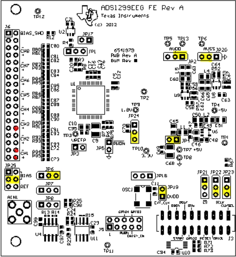
Here is the  Jumpers I set.(The red spot is bias electrode and differential measurement electrodes)

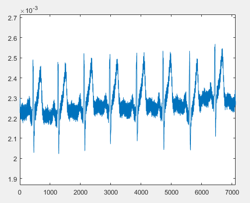
Here is the ECG and EEG I measured(1000hz)

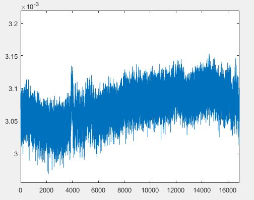
My dates have a lot noises,I wonder is there any mistakes about my configurations. 

May I ask for your help?

  • Hello,

    Thank you for your post and I'll be happy to help!

    It looks like some of your pictures did not post correctly. Can re-attach them?

    What is the frequency of the EEG/ECG signal that you are testing with?

    Looking at your register settings:

    CONFIG1 0x94 (1000Hz)
    CONFIG2 0xD0
    CONFIG3 0xE8 - The BIASREF is being generated internally, but your bias buffer is disabled. Please turn on the BIAS buffer.
    CH1SET 0x60 - PGA 24, normal input
    CH2SET 0x81 - Power down, input short
    CH3SET 0x66 - PGA 24, BIAS_DRP MUX
    CH4SET 0x81 - Power down, input short
    CH5SET 0x81 - Power down, input short
    CH6SET 0x81 - Power down, input short
    CH7SET 0x81 - Power down, input short
    CH8SET 0x81 - Power down, input short
    BIAS_SENSN 0x01 - CH1 route into BIAS
    BIAS_SENSP 0x01 - CH1 route into BIAS

  • Thank you for your reply, I'll try it,and reply you back.
  • The lost pictures. 

  • Hello,

    Thank you for providing the lost pictures. Can you provide a little background on these? What is the second picture of and why are the jumpers out of their default positions? I'm just trying to understand what you're trying to do with the device.

    Additionally, what are the rest of your register settings?

    Have you tried powering on the bias buffer as I mentioned in my previous post?
  • I tried your suggestion. The answer seems better than before.

    This is my recollected data and and a small amount of filtering.

    As for the modification of the default pin settings of the daughter board, I added the Bias electrode and removed the reference electrode.And I use the ADS1299's internal clock.

    If you want to see specific changes, I can point out to you.

  • Hello,

    I'm glad to hear that powering on the BIAS BUFFER produced better results.

    Can you explain what these pictures are?

    What are the additional register settings?

    What exactly is the problem that you are experiencing?