This thread has been locked.

If you have a related question, please click the "Ask a related question" button in the top right corner. The newly created question will be automatically linked to this question.

ADS8568: Spurious BUSY signal with Parallel communication

Part Number: ADS8568


Hi, everyone!

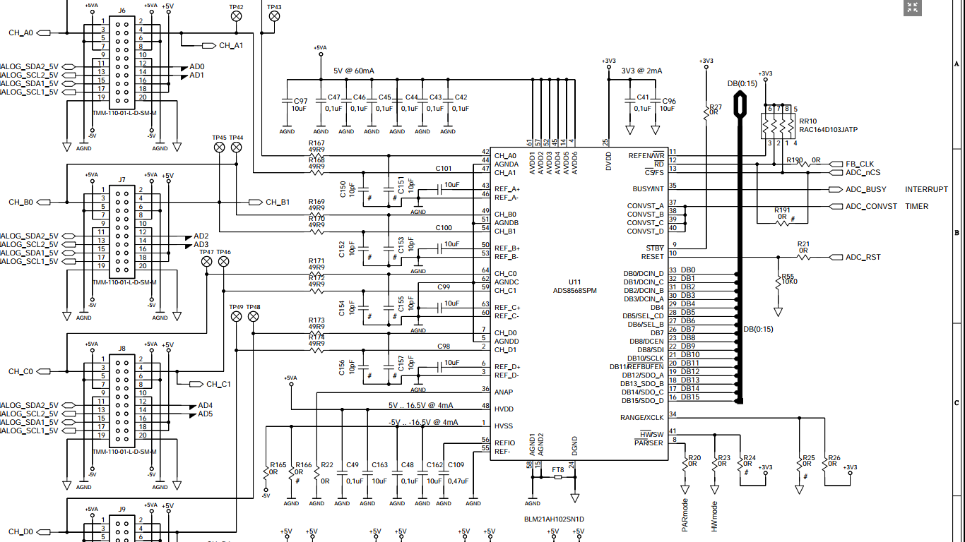
I have a custom board with an ADS8568 configured in hardware mode. I trigger the coversion with a PWM generated from a microcontroller; all 4 CONVST pins receive the same signal.

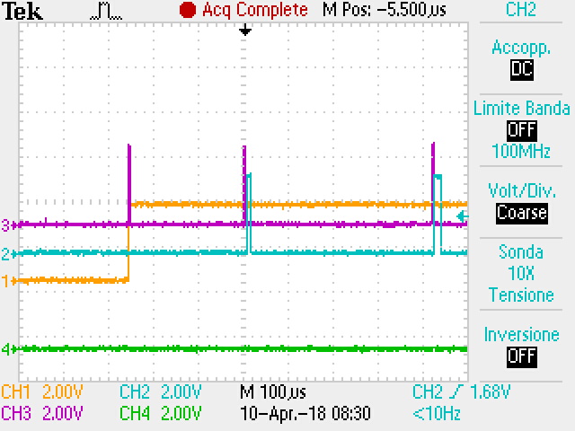
In my firmware, I check the delay between two consecutive BUSY  falling edge, and I've noticed that sometimes the delay is way lower than the PWM period.

Analyzing the problem with an oscilloscope, I've noticed that there are spurious BUSY signals not relative to any CONVST (the CONVST is clean and steep, so it is not due to noise on this signal). Debugging the problem I've noticed that the occuence frequency of these "spikes" is relate to the read frequency. As an example, reading all 4 channels, I'll get a spurious busy once every 10 seconds. If I don't read anything after BUSY falling edge, I'll get no spurious BUSY.

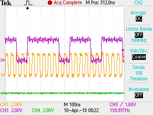
For testing purpose I'm working with a slow CONVST (50Hz). As said, ADS8568 is in HW mode, parallel interface.

Any idea?

Thanks

  • Hello Massimo,

    Can you please get a screenshot with scope for CONVST, BUSY, /CS and /RD? it will be good to have an additional zoomed-in screenshot too, please upload your schematic as well. Thanks.

    Best regards

    Dale

  • Hi Dale,

    here are a couple of screenshots.

    Blue waveform is a "software trigger"; the firmware generate a pulse when it detects a BUSY interrupt with a short delay with respect to the previous one.

    Yellow waveform is the CONVST signal. Purple line is the BUSY signal.

    As you can see, CONVST get high, and the ADC generate the BUSY signal as expected. A spurious BUSY signal is generated after ~200us, while CONVST is still high. (firmware detects the event and generates blue pulse). Another spuroius BUSY is generated after ~400us. As said in the previous post, CONVST period is 20ms.

    Blue waveform is the "software trigger", again; generated just after the spurious busy (not shown here).

    Purple waveform is the nCS signal. All 4 channels are read, with 4 16+16 bit burst. The readout always starts ~2us after the BUSY interrupt. The full interrupt routine takes about 10us to complete; just to point out that the spurious busy doesn't always happen after a parallel acces (see previous screenshot).

    Here is the parallel interface main signals. Purple waveform is nCS signal (3 16+16bit read burst are shown here).

    Yellow waveform is the nRD signal. As you can see, the nRD signal is switching continuously. I'm working with a Freescale Kinetis processor, using Flexbus interface for parallel communication. With Flexbus, the "clock" (nRD signal here) is always running. Anyway, the nCS signal that actually enables the communication with the ADC is set only during actual read.

    Side note: nWR is always high (btw, is not used in HW mode).

    This is the schematic of the ADC. Components labeled with a # are not maounted on the PCB (e.g. R191, R24, R25, ...).

    All signals are directly connected to the uC pins.

    Hope this is enough to info to have a clear picture of the issue.

    Let me know if you need any further info.

    Thanks!

  • Hi Massimo,

    Thanks for your information.

    Your connections and configurations in the schematic look fine to me only except the driving circuit, generally you need a proper amplifier and RC filter to drive ADS8568, the proper driving circuit will settle the input signal properly during the ADC's acquisition time, so you will be able to get the performance specified in datasheet, this is another topic, please refer to TI Precision Labs online training about "SAR ADC Input Driver Design" session in below link:

    training.ti.com/ti-precision-labs-adcs-intro-to-sar-adc-front-end

    In your 3rd screenshot, the timing of nCS (Purple waveform) and nRD (Yellow waveform) may gve you incorrect data, you have two nRD low pulses during one nCS low pulse.You can keep nCS low during total 8 channels data reading, or you can make nCS low for every channel's data reading, also there are timing parameter requirements between nCS and nRD, please check Figure 2 in datasheet also as below.

    Your BUSY behavior is weird, the rising edge of CONVST_x signal will initiate the ADC's conversion, the BUSY signal goes high with this rising edge of CONVST_x signal and will keep high to indicate that ADC's conversion is ongoing, then BUSY signal will return to low when the last channel pair completes the conversion cycle. Keeping CONVST_x high will not or should not have more BUSY signals, I just verified on EVM board today. Can you please check if you have any interference signal or spike on CONVST_x signal to ADC?

    Thanks.

    Best regards

    Dale

  • Hi Dale,

    Thanks for your detailed answer.

    Regarding the driver amplifier, as you can see from the scematic the analog channels' input are routed to a strip. Custom boards, with all the necessary amplifiers and filters, will be connected to these strips. I've just omitted this schematic's section, since unrelated to the problem.

    About the nCS vs. nRD timing I'll check the datasheet again more carefully.

    Regarding the main issue, well, yes, the BUSY behavior is quite funny...
    Searching for spurious spikes on the CONVST signal was the first thing I did, but I didn't find any. It is on a PCB trace, 2cm long; quite unlikely to get such a strong noise to generate a spike. Side note, the spurious BUSY can happen when the CONVST is low, too (didn't share a waveform, but I'm quite sure it happened sometimes).

    - EDIT -

    I've checked again for spikes. Again, didn't find any. From datasheet, these spikes must be at least 20ns long; we are talking about quite "long" spikes. (not that I've seen shorter ones, anyway...)

    But, I've noticed that the spurious BUSY is actually only generated when CONVST is high. So forget about my previous statement regarding spurious BUSY on low CONVST. A workaround could be to generate a really short CONVST; awfully, at the moment I can't do such thing.

  • Hi Massimo,

    The rising edge of CONVST_x signal will initiate the ADC's conversion immediately, it doesn't require longer time on CONVST_x, also the CONVST_x high will not create these BUSY output signals, I verified on EVM board yesterday, so I think the interference signal or spike on CONVST_x signal leads to this behavior on BUSY. 

    Below is my  suggestion for next step:

    1.  Fix the timing issue for nCS and nRD firstly.

    2. Take the acquisition board to a clean environment for test purpose, the input board with amplifiers is not needed to check ADC's BUSY signal. 


    Thanks&Best regards

    Dale

  • With "interface signal" do you refear to the parallel interface nCS, nRD?

  • Hi Massimo,

    The interference signal may come from your system or the environment where the system is working, I'm not pretty sure about the relationship between your incorrect timing of nCS/nRD and BUSY signal behavior, but I would like to suggest you to fix the timing issue firstly. Thanks.

    Best regards

    Dale

  • Hi Dale,

    I've modified the way the uC access the ADC. Now I read a single channel when nCS is low.

    P purple waveform: nCS. Yellow waveform: nRD.

    nRD is still running continuously.

    The spurious BUSY, awfully, is still there... And I still can't notice any spike in the CONVST signal. Here is a zoom-in of a spurious BUSY event

    Blue line: the usual "trigger", that signal a spurious BUSY event. Purple line: the BUSY signal. Yellow line: CONVST signal.

    BUSY switch to high ~20ns after CONVST rising edge. Also, a 20ns low status for CONVST is needed to trigger a measure (from datasheet); I have to be able to see such a spike with this oscilloscope configuration...

    Further test. Since, as said, the spurious BUSY happens only when CONVST is high, I'm able to increase the occurrence by rising the duty cycle of the PWM that generate the CONVST. By this, I was able to further zoom in and catch the event without using the "trigger".

    This is the normal behavior; CONVST (yellow) become high, BUSY (purple) follows after ~20ns.

    This is the spurious BUSY (purple). As you can see, there is no noise on the CONVST signal (yellow). Well, there is a really small step, but it's due to the probes (all signals "follow" the purple one a little).

    IMPORTANT NOTE: this happens on more than one board. So the problem is not due to a faulty ADC.

    !!!EXTREMELY IMPORTANT NOTE!!! While testing the behavior on several boards, I've noticed that the problem disappears when I actually connect an "analog board" (the one with the driving circuit, RC, ....) to the system. As you can see from the schematic in my second post, there are 4 strips for as many boards. I was testing the system without these boards when I noticed this behavior (I wasn't actually interested in the ADC values). By connecting just one of these board (any one), the spurious busy disappears.

    The only interaction between this additional boards and the ADC are the 2 channels with the analog data.

    So... what's happening?

    Thanks

    Massimo

  • Hi Massimo,
    Can you please make it clear for below?
    1. "a 20ns low status for CONVST is needed to trigger a measure (from datasheet)"
    2. "... are the 2 channels with the analog data."
    I think there is no any connection to ADC for you trigger signal, please correct me if my understanding for your circuit is incorrect. Thanks.

    Best regards
    Dale
  • Hi Dale,

    not sure I've fully understood your question... I'll try to answer.

    1. "a 20ns low status for CONVST is needed to trigger a measure (from datasheet)"

    Page 17 of the datasheet: CONVST_x low time, min 20ns.

    2. "... are the 2 channels with the analog data."

    As said, there are 4 "analog boards" with amplification stages, RC, and actual input analog signals. These boards can be mounted or not to the main board (the one with the ADC and the processor), via the mentioned strips. The ADC receive the amplified/filtered analog signals from these boards, and only these from the boards. So from board 1 it receive CH_A0 and CH_A1, from board 2 CH_B0 and CH_B1, ... That's it. All other ADC pins (power, CONVST, RD, data, ...) are routed in the main board. More specifically, CONVST and RD are connected to the uC.

    I think there is no any connection to ADC for you trigger signal

    If by "trigger signal" you mean the CONVST, as said it is connected to the processor. It has nothing to do with the "analog boards".

    Thanks

  • Hi Massimo,

    You mentioned that ""Blue waveform is the "software trigger, Yellow waveform is the CONVST signal" about your first graph, so my understanding is, your software trigger is created by your micro controller, I think it should not be connected to ADC also you didn't do that, and I just wanted to confirm. I would like to stop this trigger signal also use a simple nRD signal not clock to make the test simple.

    There are other tests we can do to check BUSY signal without your analog boards:

    1. Install front-end capacitors on input (C150,C151...C157).

    2. Connect your inputs to ground by TP42,TP43..TP49 or Pin 3/4 of J6~9.

    3. Measure the voltage difference between AGND and DGND, make sure it's less than +/-300mV.

    Thanks.

    Best regards

    Dale

  • Hi Dale,

    You are right, the micro is generating the "software trigger", and this signal is not going in the ADC but only on a GPIO. It is used to detect when the spurious BUSY happens. It is generated AFTER the spurious BUSY, so I highly doubt it can be the source of the problem.

    About the analog boards tests:

    1. Install front-end capacitors on input (C150,C151...C157).

    Will try this. Also, I have to check if this is actually done on the analog board.

    2. Connect your inputs to ground by TP42,TP43..TP49 or Pin 3/4 of J6~9.

    Already done by connected a jumper between the inputs and the analog ground. Still getting the spurious BUSY.

    3. Measure the voltage difference between AGND and DGND, make sure it's less than +/-300mV.

    Will check.

    I'll update you on monday.

    Thanks for your support and have a nice weekend.

  • Hi Massimo,
    Is there any update? thanks.

    Best regards
    Dale
  • Hi Dale,

    sory for the delay. I've made the requested checks yesterday in the late afternoon. With no luck in resolving the issue, awfully...

    So, the open questions was:

    1. Install front-end capacitors on input (C150,C151...C157).

    We've installed 3.3nF capacitors. Still the spurious BUSY signal occurs (and with the same frequency).

    3. Measure the voltage difference between AGND and DGND, make sure it's less than +/-300mV.

    It is just 1-2mV, so for sure less than 300mV.

    We've also tried to add a load on the +5V, -5V supply, so they have actually something to drive. Still no luck.

    For further reference, I've attached the analog board schematic. Maybe you'll notice something.

    As said, the spurious BUSY disappears by just attaching a single board to any of the 4 strips. (and that's why we lowered a little the "severity" of the issue; at least an analog board will always be connected on normal operation).

    Thanks for your support

    Massimo

  • HI Massimo,

    Thanks for your update, I will look into the detail and get back to you soon.

    Best regards

    Dale