This thread has been locked.

If you have a related question, please click the "Ask a related question" button in the top right corner. The newly created question will be automatically linked to this question.

maximum differential input

Part Number: ADS1278
What is the maximum differential input voltage for the ADS1278?
I am having a problem when the differential input approaches +VDD or -VDD. I made sure each analog input is not going below GND or over VDD.
Vref = 2.5V
VDD = 5V
Mode = High Resolution (MODE0 = 1, MODE1 = 0)
Format = Frame-Sync TDM Fixed (FORMAT0 = 0, FORMAT1 = 0, FORMAT2 = 1)

Sweeping the differential input Vin = VINP-VINN, and taking 1024 samples for each Vin, I get the following plot:

In red, I show the ideal transfer curve, and in blue my samples. In the y axis I just converted the number of counts to volts to make it easier to read.

The measured transfer curve agrees with the ideal transfer curve from  Vin = -4.84V to Vin = 4.85V. I took three samples close to the points where it fails, which is hard to see in the transfer curve plot because they are too close. But here are the histograms for the different cases when Vin is close to VDD and -VDD.

When Vin is close to -VDD, it seems that it wants to toggle between +5V and -5V, but it also shows values in between.

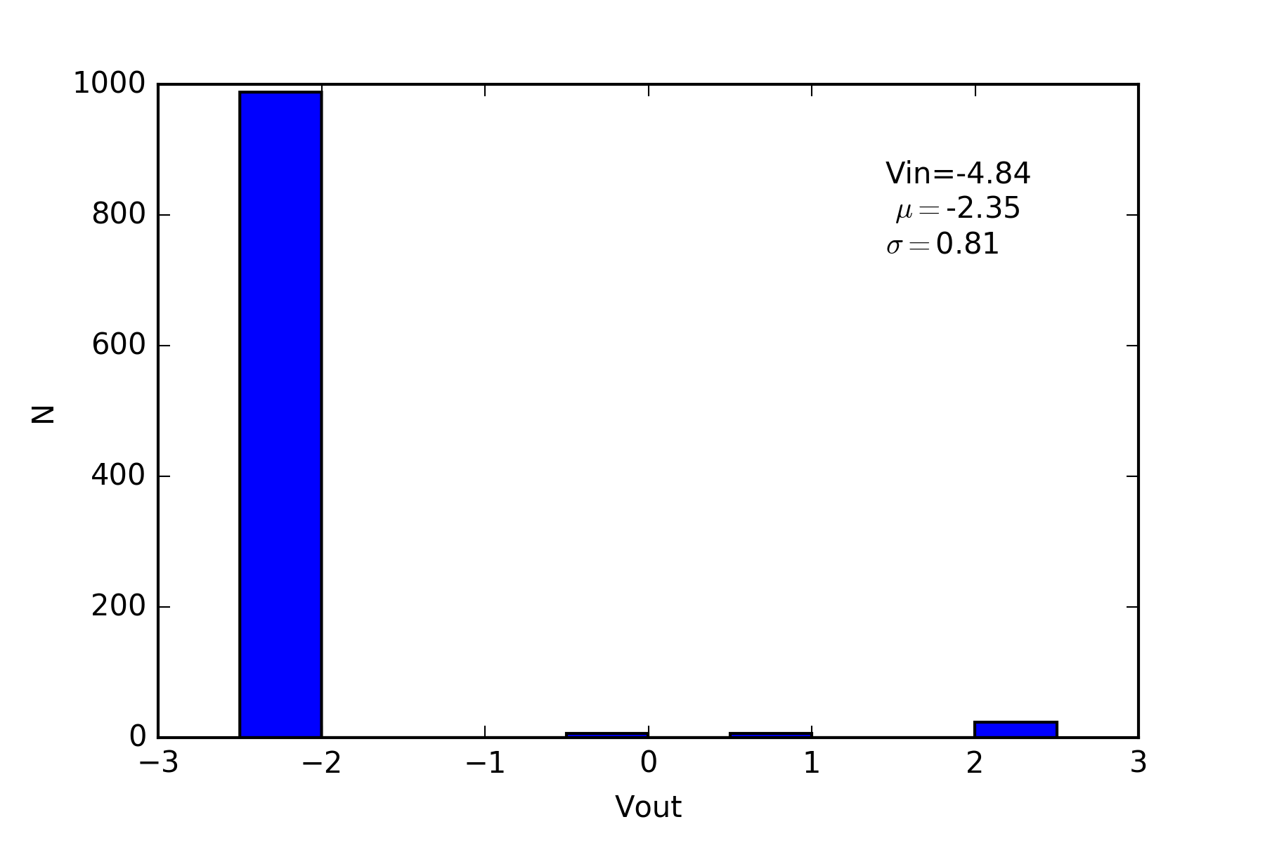
This is when it started to fail.

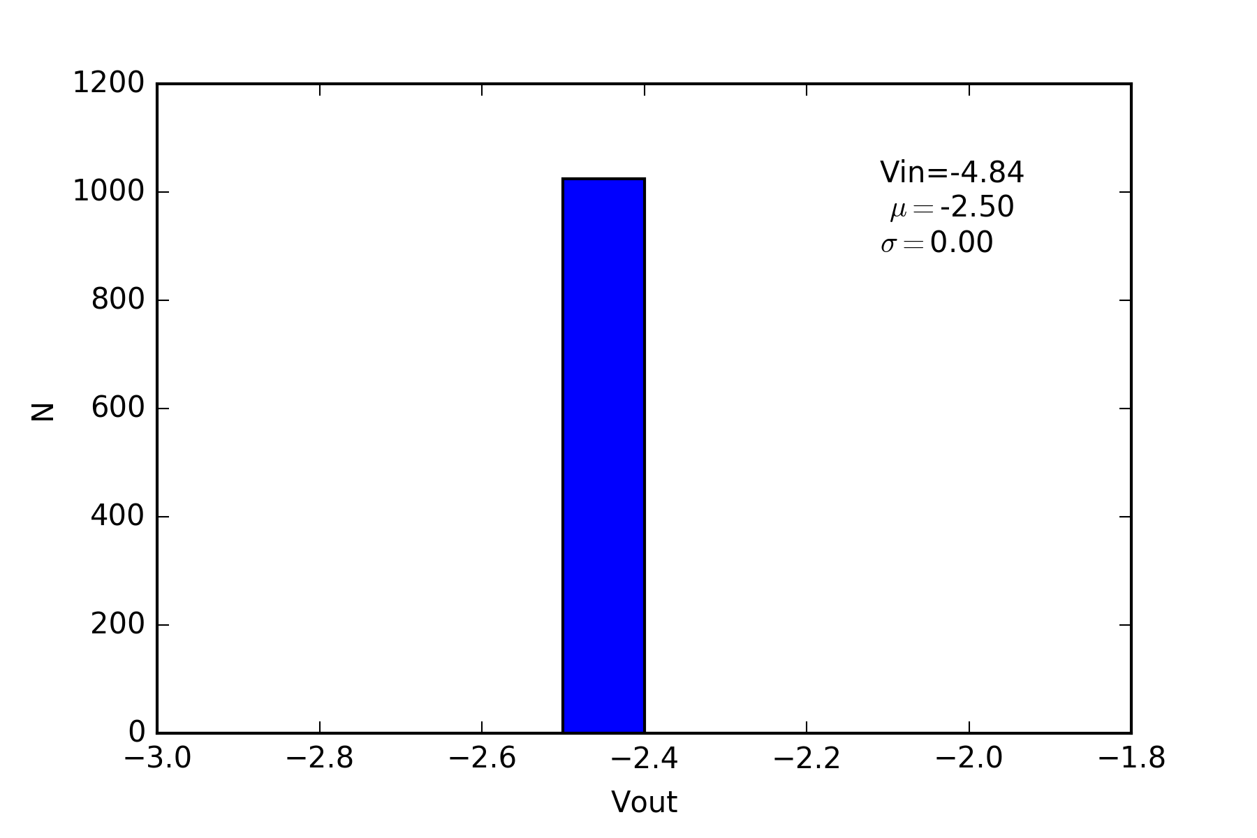
For Vin > -4.84V the ADC works perfect.

The points in the middle are fine so I will skip their histograms.
And it works good for Vin up to 4.85V.

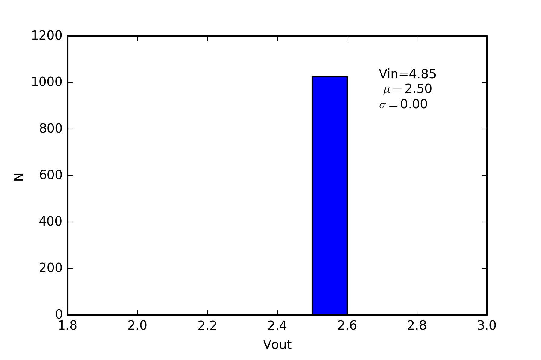
For Vin higher than 4.85V it starts to fail again, and note that the output is toggling to -2.5V when it should be saturating (clipping) to 2.5V all the time.

Here it really fails, and -2.5V gets more counts than 2.5V, even though 2.5V is the expected output.

Thanks a lot and please let me know if I need to provide more details about the driving circuit.

  • Hello Alexandra,

    Thanks for your post!

    The differential input to the ADS1278 should never exceed the reference voltage, VREF. Beyond +/- VREF, the ADC output will clip to the full-sale values shown in Table 5 below. Only the individual input pins are allowed to range anywhere between the supply rails.

    The only exception to this transfer function is when the differential input significantly exceeds VREF. As VIN approaches +/- 4.85 V, what you are observing is known as modulator saturation. This is a common phenomenon for high-order delta-sigma modulators (the ADS1278 uses a sixth-order modulator, single-bit quantizer design). When this condition is detected internally, the digital filter automatically resets until the input returns to a normal range. The output of the ADS1278 will toggle randomly between -FS, 0, and +FS (FS = full-scale). Therefore, the output data during modulator saturation should be considered invalid.

    As VIN approaches 2 x VREF, you may observe "code reversal," where the output code saturates to the inverse full-scale (i.e. +5 V input will result in 0x800000 output).

    Please ensure that the differential input stays within the expected input range of -VREF to +VREF.

    Best Regards,

  • Thanks Ryan for your answer.
    It would have been very useful if I had seen a warning about this issue in the datasheet.