This thread has been locked.

If you have a related question, please click the "Ask a related question" button in the top right corner. The newly created question will be automatically linked to this question.

ADC12DJ3200EVM: Data corruption in normal mode

Part Number: ADC12DJ3200EVM
Other Parts Discussed in Thread: ADC12DJ3200

Hello

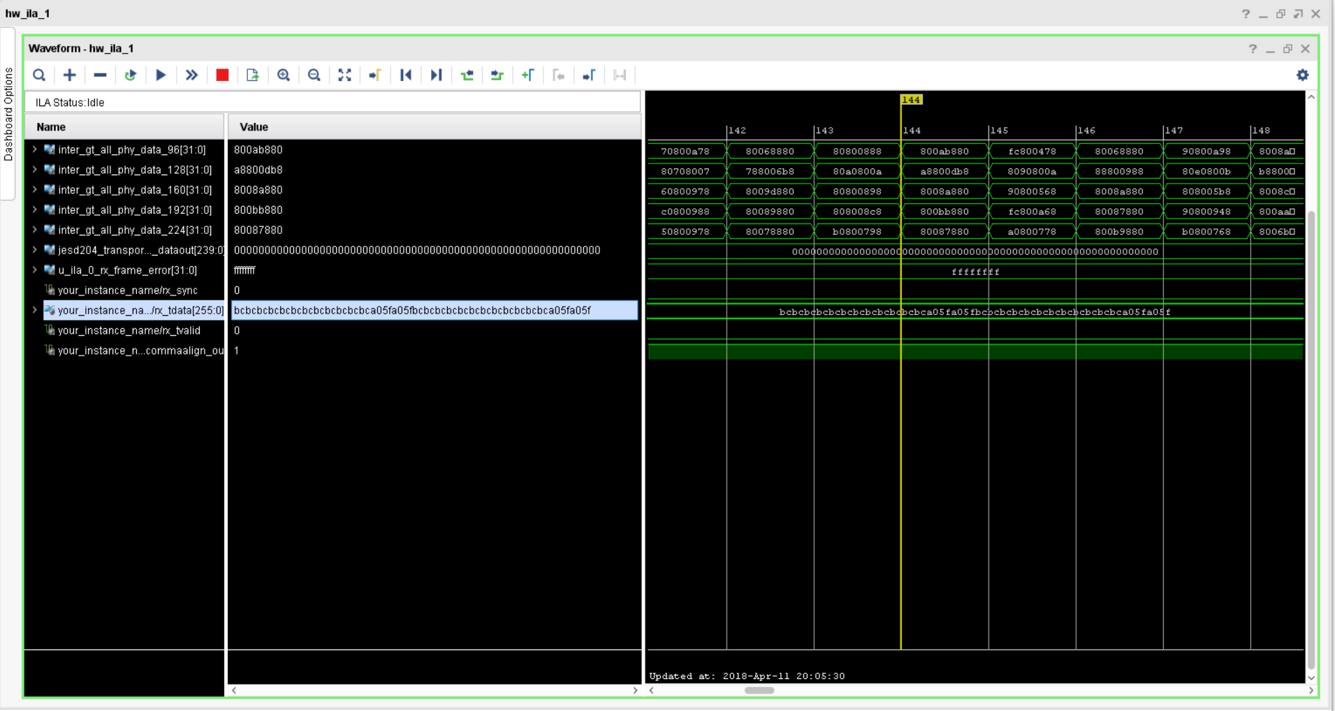
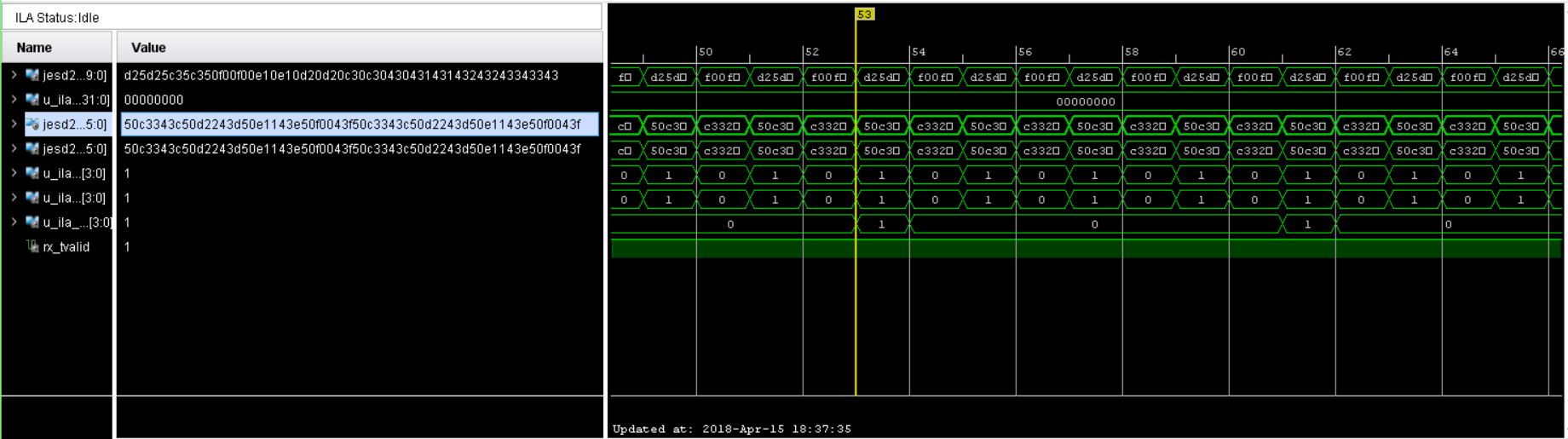
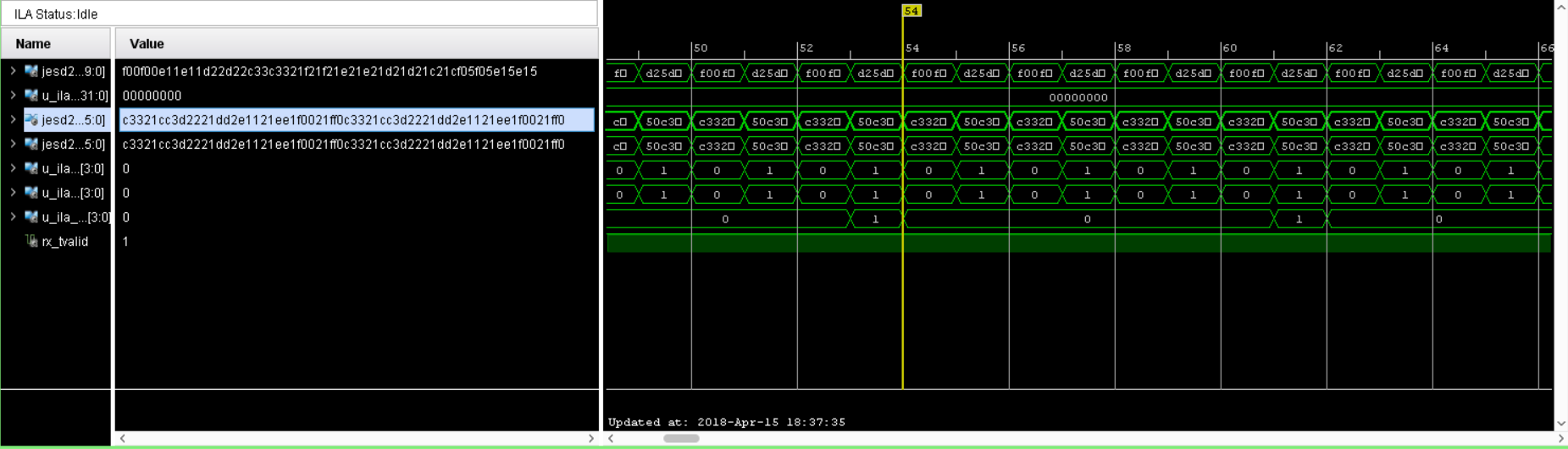
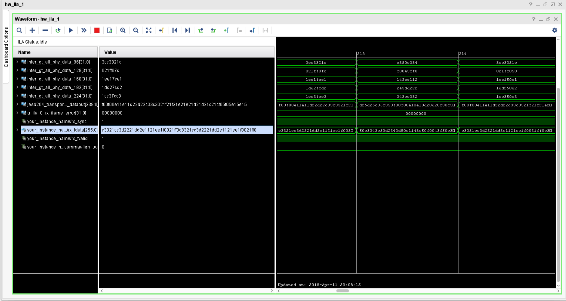
I am working with ADC12DJ3200EVM. FPGA is based on board with 8 GTX on FMC con. 

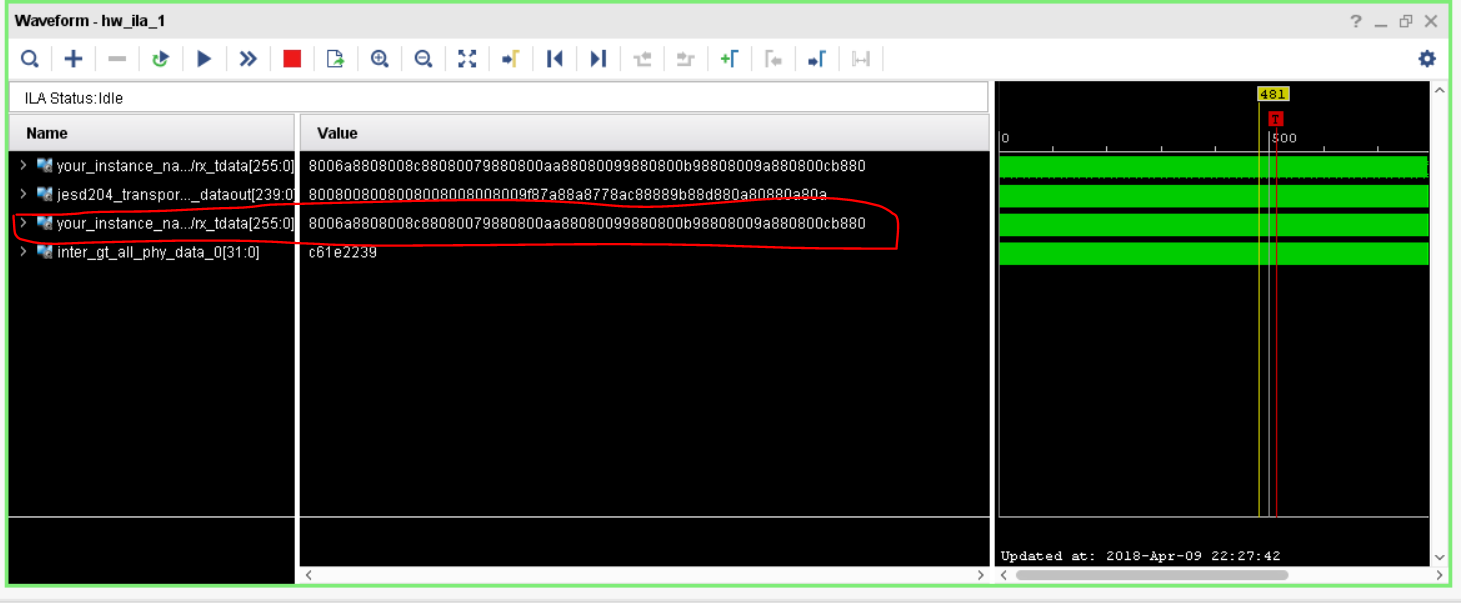
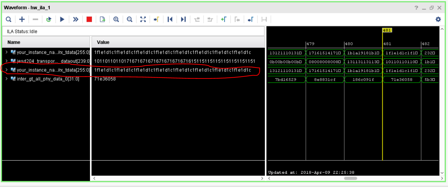
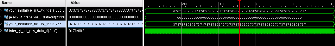
For ramp test mode I see, that data is OK. For normal mode I get wrong data (same samples are corrupted). I am using JESD204PHY and JESD204 IP (both are from Xilinx).

Settings: 4 GSPS, ref. clk = 400 MHz, Linerate = 8 Gbps, core:clk = 200 MHz. Power supply give up to 4 Amps. 

Ramp mode vs normal mode:

  • Hi David

    Please note that the ramp test mode only sends out a ramp at the octet level, not at the sample resolution of the selected JMODE.

    What JMODE are you currently configuring the EVM for?

    Do you have scrambling enabled or disabled at ADC and FPGA?

    Is your FPGA firmware compensating for the lane mapping and polarity inversions present on the ADC12DJ3200EVM?

    Here is a table showing how the lower 8 lanes of JESD204B data outputs from the ADC EVM are mapped to the FMC connector:

    DJxx O/P Lane_Num Link LID FMC Pinout TSW14J56 TSW14J57
    DA0 0 A 0 A10,A11 DP3 DP3
    DA1 1 A 1 C6,C7 DP0 DP0
    DA2 2 A 2 A6,A7 DP2 DP2
    DA3 3 A 3 A2,A3 DP1 DP1
    DB0 4 B 0 B12,B13 DP7_INV DP7_INV
    DB1 5 B 1 A14,A15 DP4_INV DP4_INV
    DB2 6 B 2 B16,B17 DP6_INV DP6_INV
    DB3 7 B 3 A18,A19 DP5_INV DP5_INV

    Can you share the data broken out for each of the 8 lanes for at least 2 frames (16 octets per lane)?

    If you aren't using it already please be aware we have an example Xilinx firmware for the KCU105 and ADC12DJ3200EVM (JMODE0 and JMODE2) available in the Tools and Software section of the ADC12DJ3200 product folder here:

    http://www.ti.com/product/ADC12DJ3200/toolssoftware

    Here is the direct download link for the package: http://www.ti.com/lit/zip/slvc698

    I hope this is helpful.

    Best regards,

    Jim B

  • I am using JMODE0.

    Do you have scrambling enabled or disabled at ADC and FPGA? Enabled

    Is your FPGA firmware compensating for the lane mapping and polarity inversions present on the ADC12DJ3200EVMYes

    Frames:


    80098880800688808009788080086880800a88808009c880800a8880800a9880

    800a988080089880800998808004788080079880800ca880800b988080099880

    808007a8808005987080099890800448a0800b8890800aa8a0800ab890800a98

    ....

    Sometimes, I get data e.g.:

    I am sorry, I do not use KCU105 board or other US or US+ FPGA. I am working with Kintex 7 FPGA (Genesys 2 from Digilent).


  • Hi David
    I'm struggling to interpret the data you have shared, both for ramp test mode and for real data mode.
    In the ramp data example you sent it looks like data from multiple lanes is combined into a single stream in the chipscope capture.
    Can you send a chipscope capture with a dedicated row of data for each lane of RX data?
    In that format, I expect each lane to show the increasing ramp pattern, with perhaps some offset in timing between the lanes.
    Also in that format, it should be much easier to find the 0 nibbles corresponding to the Tail bits that occur at the end of each Frame.
    It would also be useful to enable the Transport Test Pattern. This will send a very specific pattern of data on each lane that should help us debug what is happening.
    Best regards,
    Jim B
  • Thank you for your time and help.

    Link parameters: K = 4, Scrambler off, JMODE0, Sample rate = 4 GSPS, ref. clk = 400 MHz, LineRate = 8 Gbps, core_clk = 200 MHz, SYNC: TMSTP is used. 

    There is very often problem with Frame Error.

    Normal_data (Frame Error = 0):


    Normal data (Frame Error = FFF...):


    Transport test mode:

    I have one more questions, can you tell me -  is there a problem with Export restriction to EU ? Actually we use ADC from AD, but only ADC12DJ3200 has a good Sample Rate for our purpose (civil use).  I think only ICs (ADC12DJ3200, LMX..., LMK..., etc.), not EVM boards. 

  • Hi David
    I'll review the latest data today.
    I'm not aware of any issues with export restriction of this product to the EU.
    I recommend contacting your Texas Instruments distributor regarding the specific component or EVM part number to confirm availability.
    Best regards,
    Jim B
  • Hi David

    The data with transport test mode enabled is the most useful.

    It appears that data is coming through correctly but it is hard to interpret for the following reasons.

    1: I see the repeating pattern in the frame, but the start and end of frame data are not aligned in the 32 bit data blocks.

    2: Within each 32 bit block of data, the 8-bit values (2 hex codes) are rightmost, and the later ones are to the right. So it is confusing to re-order into the proper sequence.

    If I look at the 2nd row down, this corresponds to the expected data for lane DA0 or DB0. The first 12-bit value expected is 0xF01. So we need to find F0 in the data, with 1F to the left of it (later in time). This occurs in the middle of the first block of data.

    I'll retype all 3 blocks and then re-arrange for clarity:

    021FF0FC F0043FF0 021FF050

    Starting at the highlighted characters and working left within that block we get:

    F0 1F 02 then starting at the right of the next block we have F0 3F 04 F0 then 50 F0 1F 02

    Grouping together into 12 bit values we get:

    F01 F02 F03 F04 F05 0 F01 F02 

    The highlighted 0 is the 4 tail bits at the end of the frame. The other lanes look similar.

    The only anomaly from the expected transport test pattern data is that we see FC occuring in some locations. Those values are the JESD204B frame alignment monitoring character (K28.7) that are inserted into the data stream as expected according to the character insertion rules with scrambling disabled. You may also see 7C (K28.3) multi-frame alignment character appearing for similar reasons. The JESD204B receive IP should handle these characters and replace them with the appropriate values according to the same rules. This is discussed in section 5.3.3.4.2 of the JESD204B.01 specification. Xilinx should be able to help you if there aren't being handled correctly.

    I think these same characters not being handled correctly may be causing the Frame Error = FFF... in the Normal data capture you provided. 

    I hope this is helpful.

    Best regards,

    Jim B

  • Hi Jim
    thank you for your anylysis. I will try solve this problem with Xilinx.
    Have a nice weekend!
  • Hi Jim
    I would like return to your analysis. Did you analyze data from PHY layer (inter_gt_all_phy)?

    Because these data goes from PHY layer (before RX core with character replacement), so the character such as K28.7, etc. are expected, or not?

    The output from RX core is named your_instance_na... (highlighted row), on RX core I do not see K28.7 symbols. Sorry for mystification.

    EDIT:

    I think that there is a problem with errors in  the bit order. instead of a problem with character replacement. 

    TRANSPORT LAYER:

    first half of frame:

    second half...

  • Hi David

    I only analyzed what I was seeing in the PHY layer. The information I'm seeing there looks correct. The alignment characters are expected to appear there, but should be replaced by the JESD204B IP.

    I don't understand the information in the highlighted row in the 2 TRANSPORT LAYER images above. It looks like information from all 8 lanes is combined together into that output, which is not what I'm expecting to see. If you're not getting the correct results at the output of the RX core then I think it is either not configured correctly, or there is some other problem.

    Regards,

    Jim B

  • Thank you for the clarification and your advice.