This thread has been locked.

If you have a related question, please click the "Ask a related question" button in the top right corner. The newly created question will be automatically linked to this question.

ADS1247: ADS1247 Output data is varying every time i reset/power on

Part Number: ADS1247

Dear TI team,

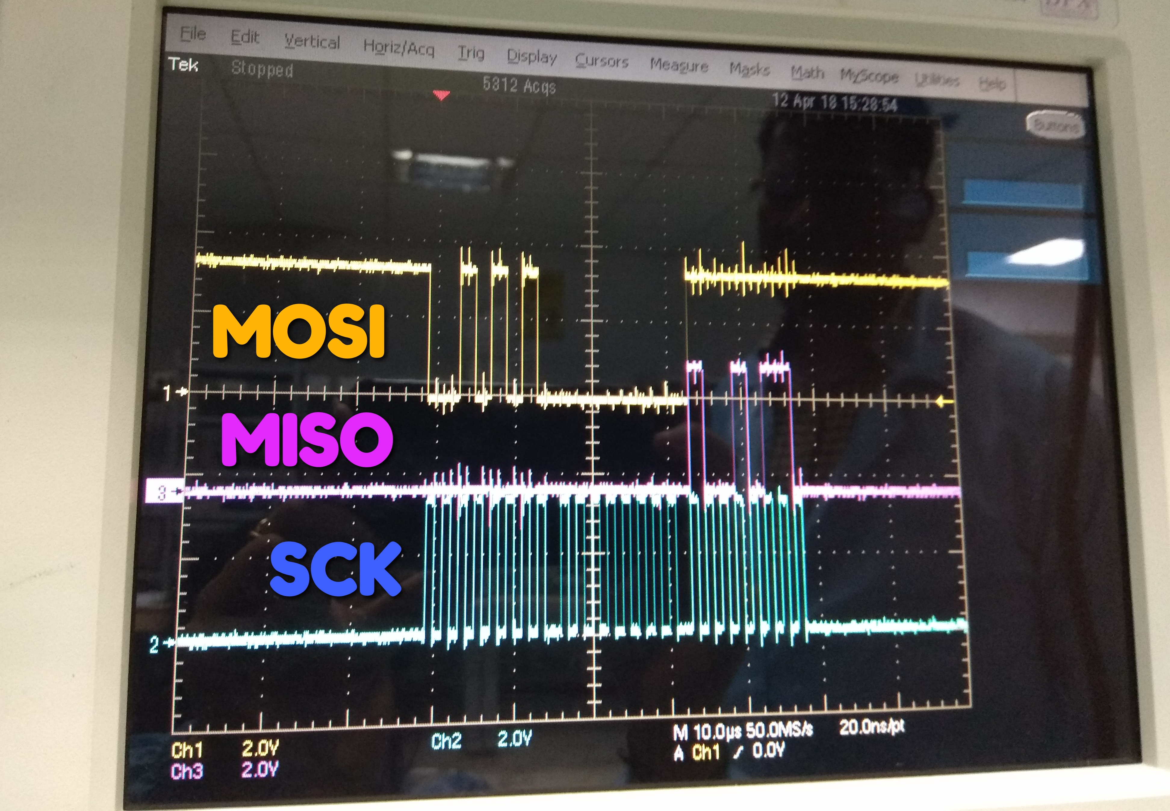
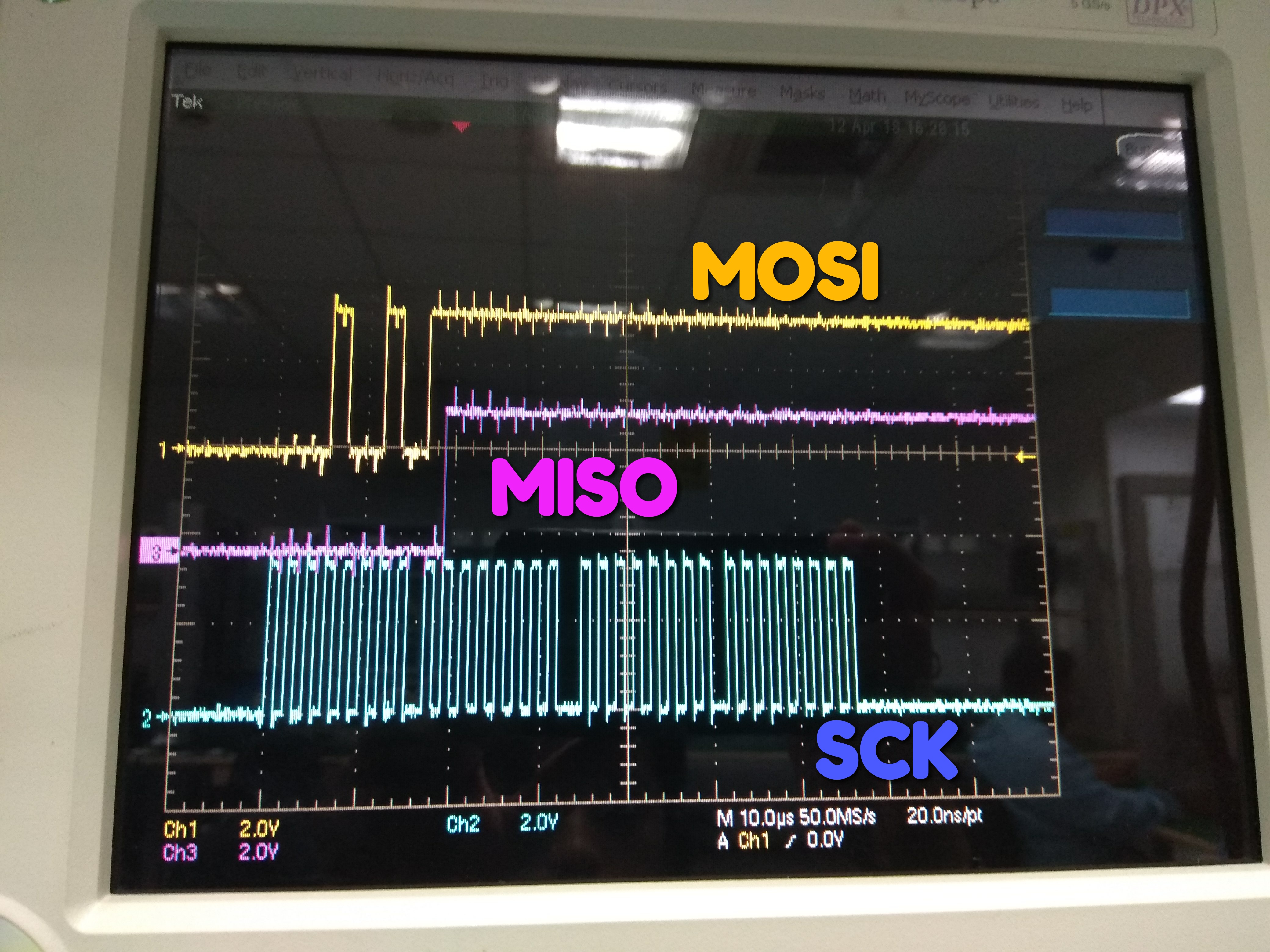
I am communicating with ADS1247 using ATmega128 (SPI mode1, 1MHz clock, MSB first).

I have used 3 wire design example as per the datasheet and also done register configuration as in datasheet.

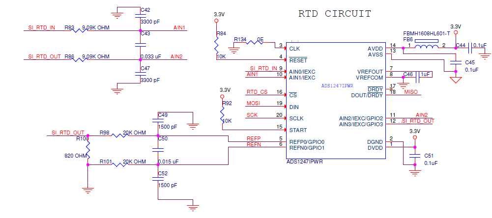
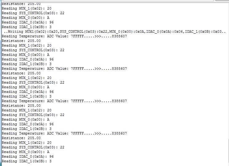
I was getting only 7FFF (Sending RDATA, NOPs & reading data in a loop) . Also the voltage across RREF(R100) is 820 mV.

I tried changing gain & sampling rate, SPI clock rate settings. But the result is same :(

Then i started reading data by checking DRDY status (Configured for DOUT/DRDY). Now I am getting constant value (not correct), but varies after every power on/reset.

Reference voltage across 820ohm is still 820mA.

Thanks,

Sushma

  • Sushma,


    What values are you getting and how much variation are you getting with each power on/reset? Are the values close to expected or are the very far off from what you think you should get? The resulting values might be due to some settling in your circuit. If you have output data, I would like to see the raw data from the ADC and I will need more information about the setup.

    Based on the labeling on the schematic you show, it looks like you are making a 3-wire RTD measurement. The ADC inputs are set to AIN1 and AIN2, while you use two current sources at AIN0 and AIN3 to drive the RTD. The two current sources are summed into the reference resistor (R10, 820Ω) which is the reference. The schematic basically looks correct, but let me know if there are any changes or unpopulated components.

    If the errors are extremely large, you'll need to verify the setup. It looks like you have made measurements on your circuit with a multimeter, but if not, verify that 1. VREFOUT to VREFCOM is 2.048V to enable the IDAC currents; 2. that you have the proper voltage across the reference resistor (0.82V if IDACs are 500uA or 1.64V if IDACs are 1mA); 3. the voltage across the RTD is correct (IDAC current x ~100Ω if it is a PT100 RTD - you can measure it across C43 and report it back); 4. the voltage across the reference resistor is correct. I would also check to see that /RESET and START are both high and the the supply voltages are correct.

    After that, how do you have the ADC configured? I need to know settings for the input pins, data rate, PGA value, IDAC settings, IDAC outputs, VBIAS settings and burnout current sources. It very is important to read back all ADC configuration registers. By reading back the ADC configuration registers, it shows if you've written to the device correctly.

    If the errors are smaller, then this could be some settling in the circuit. How much time is there from the start time to the configuration of the device, and how much time is there from the configuration of the device to the first data read. There will be settling as the IDAC currents turn on and the external circuitry settles. There will be some time for the VREFOUT to settle. As the IDAC currents turn on, there will also be time needed for the capacitance from the filtering of the input and the reference to settle. This would be from C43 and C50. With large series resistors (R83/R86 and R98/R101) you may need several milliseconds to settle.


    Joseph Wu
  •  Hi Joseph,

    I am getting random values like 7FFFF(Most of the times),0,FFFFF,FFFFE,...

    For testing I have connceted a fixed 120ohm resistor between AI_RTD_IN and SI_RTD_OUT

    Yeah..I have measured the voltage using multi meter.
    1. VREFOUT to VREFCOM is 2.048V
    2.voltage across the reference resistor=821.4mV (IDAC set to 1mA)

    3.Voltage across 120 ohm(used for testing)= 0


    ADS1247 configuration:-
    CS\ low,5us delay
    RESET, 0.6ms delay
    SDATAC, 210ms delay
    MULTIPLEX_1: 0x20
    SYS_CONTROL:0x22
    MULTIPLEX_0:0x0A
    IDAC_0:0x06
    IDAC_1:0x03
    10us delay
    CS\ high

    SPI settings:- RTDSettings(1000000, MSBFIRST, SPI_MODE1)


    To Read data : -
    CS\ low,5us delay
    RDATA
    RTDvalue |= SPI.transfer(NOP);
    RTDvalue <<= 8; //First byte is MSB so shift left 8 places
    RTDvalue |= SPI.transfer(NOP);
    RTDvalue <<= 8;
    RTDvalue |= SPI.transfer(NOP);

    Serial(RTDvalue)

    5us delay

    CS\=HIGH


    I am calling ReadData function in loop with 500ms delay.

    I read each registers (using RREG) and got correct values (the values i have set).


    Thank you,
    Sushma

  • Sushma,


    There are a few things I'd like to point out in your last post.

    First, 7FFFFF is not a random output. That value is a positive full-scale measurement. This could mean several different things (the input is much larger than expected, the gain is too high, the input is disconnected and has floated to a large value, or it could mean the reference is 0 or much lower than expected).

    Second, if you've copied the design from the ADS1247 datasheet, the voltage across the reference resistor should be 1.64V not 0.82V. This is shown in equation 26. There are two IDAC current sources, with one going into first lead of the RTD while the other goes into the second lead of the RTD. Both currents are summed and leave the RTD through the third lead and both drive the reference resistor. The principle of this is shown in Figure 116.

    I think that you have a bad connection in the RTD test for the second IDAC current because your numbering is a bit off. If you're getting some 0 data, then I think your other RTD connections might be bad. However, starting with the first data, you get 499BE0.

    499BE0h = 4824032d

    If you ignore the second IDAC current and only current from IDAC1 is entering the RTD, then you have basically the correct value. The RTD resistance is calculated:

    RRTD = 4824032 * RREF / (Gain * 2^23) = 4824032 * 820Ω / (4 * 2^23) = 117.89Ω

    This value is close to your expected value of 120Ω. However, this measurement includes some lead resistance from the RTD. As explained earlier, you would have two IDAC currents driving different leads of the RTD, so the calculation would have been:

    RRTD = Output code * RREF / (2 * Gain * 2^23)

    This is because the reference voltage is twice as large, because there are two IDAC currents. I'll note that your measurement is a bit off from expected. This could be because your test RTD measurement is off from 120Ω or the reference resistance is off from 820Ω. If you want a precision measurement, both values need to be low in error. Also, if you want a very accurate measurement from this 3-wire measurement, you'll need to swap the outputs of the IDACs and take a second measurement to average. This will remove the error from the mismatch of the IDAC currents.

    Read through these comments and the application design in the datasheet carefully. Then check the connections of the RTD and the board. You should be able to get the correct output from the ADC.


    Joseph Wu
  • RTD TESTING.pdf

    Hi Joseph,

    Thank you for the reply.

    Yeah, I have taken design and register settings from the ADS1247 datasheet only.

    Now i am using RRTD = Output code * RREF / (2 * Gain * 2^23) for resistance calculation in my code.

    I have configured for 2 IDAC currents for 1mA, but still the reference voltage is halved (0.82V). I am not able to decode this behavior.

    If I configure alone for AIN3 as second IDAC source, then also am getting the same result.

    If I configure AIN3/AIN0 as first IDAC source and disconnect the second source then I am getting random values. Please find the attached file for the same.

    Now I have doubt on first IDAC source configuration. 

    I want to know,

    1)What shold be the Spi clock frequency for 20sps sampling rate?

    2)Should I need to drive only one IDAC source? 

    3)Can I use a fixed resistor for testing in place of RTD (I have used pot also, but got the same result)?

    4) Do I have to give any specific amount of delay between any SPI commands?

    Thanks,

    Sushma

  • Sushma,


    If you are able to read back the registers and the registers are correct, there's no reason the IDAC current shouldn't both come out at the proper pin output. If you can, you could remove the reference resistor and the RTD connections and put a 1kΩ resistors from AIN0 to ground and AIN3 to ground just to see that the current comes out. I would guess that this is a bad connection or solder joint. However, I can't see and evaluate your circuit.

    When it comes to the variable output data values, this could be the same problem as I've just mentioned where there's a bad connection, or it could be a problem in timing of the conversion or communication.

    Do you set the configuration register and then make multiple readings when the device is continuously converting? Or do you use the START pin to start a single conversion and then use the START pin to take later single conversions. Also when you read data, do you use the device in SDATAC mode and use RDATA to get the conversion data, or do you have the device in RDATAC mode and just use SCLKs to get the data. The point is that when you take the data, you don't want a new conversion to interrupt the data read with new conversion data.

    It may be worthwhile to use an oscilloscope or logic analyzer to check the data coming out of the ADC and look at the /CS, DOUT, SCLK, and DIN lines (maybe /DRDY also). I would check that the data is coming out uninterrupted from a new conversion (by checking against the /DRDY).

    Regardless look through my comments. Here are the answers to your questions:

    1. The SPI clock frequency specifications are linked to the master clock used for the device. The min SCLK period is 488ns, assuming that the master clock is 4.096MHz. That's an equivalent of 2.049MHz. If the internal oscillator is being used, there's a variation of about ±5%, so the max would be about 1.497MHz. If you're using an SCLK of 1MHz, none of this should be a problem.

    2. You could drive the RTD with a single IDAC, but the way that you have the circuit set up, you cannot eliminate the RTD lead resistance as an error source. There are alternate topologies to measure a 3-wire RTD with a single IDAC but it takes to measurements to measure the RTD+lead wire resistance, and then measure a second lead wire resistance to cancel. Unfortunately, with this circuit configuration, I don't think you can make the second measurement.

    3. You can certainly use a fixed resistor instead of a pot. The data in the example design comes from using a set of precision resistors connected up like a 3-wire RTD.

    4. For you case, the only timing information that is necessary is listed on pages 11 and 12 of the datasheet. If you were running at 2kSPS for a data rate, there is other timing requirements for SCLK to get single cycle settling. If you are concerned with communication timing, I'd recommend the oscillator/logic analyzer readings and post the results as I mentioned in the previous section.


    Joseph Wu
  • Hi Joseph,

    Sorry for the delay.

    >when you read data, do you use the device in SDATAC mode and use RDATA to get the conversion data

    Yes. Before configuring ADS1247, am sending SDATAC and then am calling RDATA followed by 3 NOPs in a loop.

    I read back the registers and the registers are correct. 

    Serially printed raw data:

    IDAC_0 =0x96, because it includes device ID also.

    ADC value (temperature value) is 0x7FFF. 

    I verified the current value and I am getting both the currents (IDAC0&IDAC1) at AIN0&AIN3 respectively. But am not getting 0.12mV(IR=1mA*120ohm) voltage across 120ohm(used for testing).

    DRDY\ pin is not connected to micro controller. I captured /CS, DOUT, SCLK, and DIN lines in oscilloscope. CS\ remains LOW only.

    Then I modified the code to read only temperature data (RDATA&NOPs) , removed RREG part. I was calling function to read temperature in loop with 1s delay.

    Thank you,

    Sushma

  • Sushma,

    I've looked through your last post, and the register values that you are able to read back seem correct. MUX0 is 0A for using AIN1 and AIN2 as the inputs, MUX1 is 20, always enabling the internal reference, setting the reference to REFP0/REFN0, with the device in normal operation. SYS0 of 22 sets the PGA=4 at a data rate of 20SPS, IDAC0 of 06 sets the IDAC current to 1mA, and IDAC1 of 03 routes the currents to AIN0 and AIN3.

    At this point, I still think you have a bad connection somewhere. This is what I think it looks like.

    If the test resistance that you're measuring is broken where the red x's are, you'll get results similar to what you're getting. IDAC1 is trying to route 1mA to the RTD resistance, but it doesn't get there, pulling up on AIN1 to near AVDD. IDAC2 properly routes current to AIN3, but since IDAC1 does not reach RREF, the voltage at AIN2 is only 0.82V. With AIN1 near AVDD, the voltage from AIN1 to AIN2 is much larger than the full-scale. This gives an ADC reading of 7FFFFFh. At the same time if you measure the voltage across RRTD, you get a voltage of 0V because there's no current across it.

    There are several things you can do to debug the circuit. You can try making an ADC measurement from a different location. Measure AIN0 to AIN1 or AIN2 to AIN3 to see if they're still connected. You can also reroute the IDAC currents to different pins to see if the current from IDAC1 comes out somewhere else. Using a voltmeter or ohmmeter to check the circuit would certainly help.

    Regardless, can you please post a closeup picture of your circuit and the front end. There might be something that I can see that you can check.

    Joseph Wu

  • Sushma,


    One thing that I just noticed was the inductive filter for the supply. This would be the FBMH1608HL601-T attached to AVDD. I think you should remove this and replace it with a short. Because the ADC has digital currents (and other switching currents with the analog supply), the inrush currents can be large. This will cause large ripple voltages because of the L(di/dt). In this case, it is also complicated with the fact that the filter has a 600Ω series resistance.

    It's possible that this inductance could cause a device reset. When first powering it on, and enabling the reference, the in-rush current could be large. This could cause a power-on reset to occur because the supply voltage may have drop below the allowed supply.

    Regardless, I would remove the inductor and short the leads.


    Joseph Wu
  • Sushma,


    I haven't heard from you for a while and I wanted to know if you had checked your circuit and made adjustments based on my previous two posts. I think the inductance in the analog supply line is a potential problem.

    If you've figured out your problem, great. If not, please post back and we can discuss your circuit further. Regardless I'll close out this post. If you have more questions, you should be able to post back to this thread.


    Joseph Wu
  • Hi Joseph,

    Thank you so much for the help.
    Its my bad that i didn't check the resistance (120ohm) pin connection. It was soldering mistake. After that I am getting output.
    Sorry for the trouble.

    Sushma
  • Sushma,


    I'm glad that you were able to get the circuit to work properly. I thought it was likely that there was a bad connection on the board based on your data. Data appeared to show that there were intermittent points where the inputs were completely open, inputs working but missing the the first IDAC current, and cases where the board seemed to be working. It all pointed to some problem in the board connection.

    If you have any further questions feel free to post back to the forum.


    Joseph Wu