Other Parts Discussed in Thread: OPA1678,
Please let me know about three points below for ADS131A04 setting.
①Negative charge pump output(NVCP)
If VNCP unused, is VNCP really connect AVSS, OK?
EVM user's manual P16 is described that JP8 should to connect after setup.
Is this condition only the case of use NVCP?
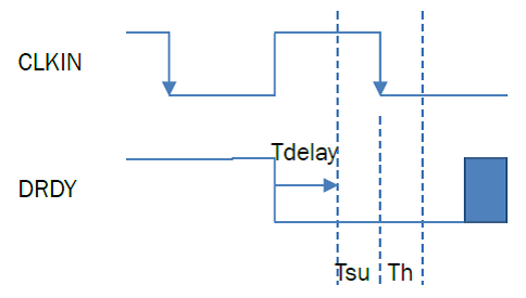
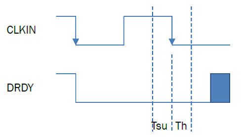
② Timing for /DRDY and clock (CLKIN or SCLK)
Please let me know about recommended timing for /DRDY and clock.
Customer is worry about metastable,
・This case is /DRDY made by CLKIN rise, but the margin of Tdelay is small.
・This case is /DRDY made by CLKIN fall, but I think possibility of metastable.
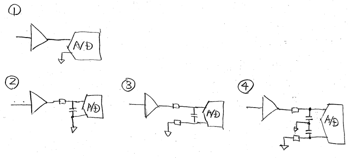
③Input connection
If ADS131A04 input side(AINx) is connecting OPA1678, is RC filter necessary to connect between OPA1678 output and ADS131A04 input?
Or is direct connection no problem?
Best regards,
Satoshi