This thread has been locked.

If you have a related question, please click the "Ask a related question" button in the top right corner. The newly created question will be automatically linked to this question.

ADS1220: Calibration : Can't get precise ADC 24bits data based on the 3 wines RTD design of TIDU271

Part Number: ADS1220

Hi all,

This is my first question on the TI forum, so maybe I will break some rules ?LOL 

Here is my Circuit schematic , I have combined the design of the datasheet ADS1220 and the design shown on figure40 page 33 of TIDU271

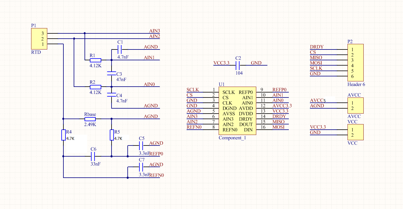
The compoments selected for the fliters of VIN and VREF are based on the data shown on page37,38 of TIDU271

The SPI channel is connected to a MCU STM32F103.

The registre setting is 66h 04h 55h 70h .

I can change the value of VREF(mesuring by a voltmetre) by changing the registre setting(value of IDC), I think it means the SPI connection works well.

The MCU can receive the 24 bits data converted by ADS1220.

There are 3 problems

1 : figure40 page 33 of TIDU271 shows that we can supply VDCC of ADS1220 by 5 volts , but in fact , the SPI connection will never work while using 5v VDCC , it only works on 3.3v VDCC.

2 : When the MCU restart , the 24 bits data received will be "abnormal" ,always 0x7FFFFF or 0x800000. To return "normal" data , il takes a while to wait or I can disconnect the PT100 and reconnect it.

3. The offset is not stable , here is the table I have mesured with a calibrated temperture equipment (the calibration of this equipment maybe not good enough to provide a well temperture)

Temperture 50 60 70 80 90 100 110 120 130 140 150
Standard 1608995.65 1660742.25 1712488.84 1763965.92 1815308.25 1866515.81 1917453.87 1968391.92 2019060.46 2069594.24 2120128.03
Mesure 1551952 1602620 1652042 1702369 1751886 1801365 1851184 1900589 1950509 1997712 2046000
Offset 57043.6549 58122.2489 60446.8428 61596.9232 63422.2469 65150.8138 66269.8672 67802.9206 68551.4605 71882.2436 74128.0267

Design of 3 wines RTD in datasheet of ADS1220 shows that it only needs a offset calibration when PT100=100 ohms ,but the data shows that the offset will increase when the 24bits data increase.

The 24-bits data received by the MCU is also unstable,the data will change randomly(with a offset about 5-6 degrees) while light touching the circuit(like the pins of PT100).

Cordialement

SITU

  • Hi SITU,

    Welcome to the E2E forum!  Let's start with the schematic first.  You have a supply decoupling cap on the digital supply (C2), but you should also have one on the analog supply as well.  For the RTD circuit to the ADS1220, there is an issue with the reference connection and how the reference is connected to the RTD.  The net labels REFN0 and REFP0 are incorrect and should be swapped.  You want the REFP0 connection to be connected to the junction of R4 and C6.

    Regarding 1: It is possible for the ADS1220 to be connected to 5V, but many microprocessors will not accept that high of voltage.  In this situation you can supply both voltages with 3.3V, or you can set the DVDD supply to 3.3V and the analog supply to 5V.  Analog and digital grounds should be connected together near the ADS1220.

    Regarding 2:  When powering up the system, you must wait a period of time before attempting to communicate with the ADS1220 after both analog and digital supplies have reached the nominal voltage levels.  Be careful not to apply any voltages to the digital input pins until after the DVDD voltage has reached the nominal operating voltage.  To know for sure whether the ADS1220 is ready to go you can monitor DRDY.  When powering up the DRDY will go high and the device will complete one conversion and go to a low power mode after setting DRDY low.  At this point you can safely communicate to the device (approximately 50ms after power up).

    Regarding 3: You must properly connect the device before you can get meaningful readings.  All your readings show negative values.  Positive full-scale is 0x7FFFFF and negative full-scale is 0x800000.  A -1 code is 0xFFFFFF.

    You need to make sure that your measurement is using the REF0 input pair, and that you have determined both offset and gain for your calibration.  What you are calling offset error is actually gain error.  The offset error can be determined by using the internal short of the ADS1220, and the value of this should be subtracted from the results.  Once you have adjusted the offset error from the result, you can determine the gain error by connecting the 100 ohm precision resistor to the input and determine the gain factor.  This factor is then multiplied by the offset adjusted result.

    In the end, the code value returned should be a ratio of the resistance of the reference resistor to the RTD.  Take a look at the RTD example in the ADS1220 datasheet.

    Best regards,

    Bob B

  • Hi Bob !

    Thank you for your reply.

    For the first problem (SPI connection with DVDD 5v), I have read the datasheet of STM32F103 , the pins for the SPI1 channel are not 5V tolerence. It's the MCU problem .

    For the second problem ( get stange data after restarting the mcu) ,after swaging the REFP0 and REFN0 into right setting, the problem get solved. I think it's a mystery error casued by wrong reference input.

    For the third problem , I followed your suggestions about calibration , the data recevied become more stable , but still , there will be a drift about 1-1.5degrees

    For reducing the drift , there is still one more question.

    I find a structure in the design TIDU271 page , I can't understand the theory of this. Can this diode bridge work as a stablizer for the input of VRRF or VIN?

    Cordialement

    SITU

  • Hi SITU,

    The diodes shown (D6 and D10) are for extra protection from EMI. The diodes can help with overvoltage conditions with transients, but they will also provide a leakage path which can negatively impact the measurement if the leakage is too large. These particular diodes can leak as much as 100nA, which is quite significant for a current excited measurement.

    As to what you are seeing regarding the drift, it would be helpful to see a series of raw data from the ADC without any conversions. It would also be helpful for me to see the changes in your schematic following my original comments. Also please send me the register settings being used.

    Consider any self-heating affects from the IDACs through the resistors. Can you tell me the characteristics of the resistances being used with respect of tolerance and temperature coefficient? This would be for your test resistor and your reference resistor.

    Thanks,
    Bob B
  • Hi Bob ,

    I don't have a good enough resistance for calibration, i have tried a resistance-box.

    After using the single-shot mode and duty-mode ,  the drift probleme looks better .

    Sorry for replying late because i was thinking about a "upgraped" version of the design.

    There is a few more question , in the design tidu271, I find that the pins AIN3,AIN2,REFN0,REFP0,AIN0,AIN1 are connected with a 249 ohms resistance.

    But doing this will make the error become large , so I repalce them with the 0 ohm resistance. what's the fonction of these 249 ohms resistances , is that work after the replacing?

    Cordialement

  • Hi SITU,

    I would suggest you try to follow the input current paths of the tidu271 design. This design is not a simplified design, but rather one that is designed to pass certain IEC tests. In particular look at Figure 52 on page 42 which shows an example of the protection circuit used. The 249 ohm resistors are for current limiting after all other circuit protection has been activated. D19 and D20 are for limiting electrical fast transients (EFT) from ESD or other similar events. D18 and D21 are for limiting any high or overvoltage conditions at the input terminals.

    The 249 ohm resistors are not used in the IDAC current path for supplying the excitation to the RTD. Instead diodes are used to limit reverse current back into the ADS1220.

    As far as drift, using Single-Shot mode and/or Duty-Cycle mode should not make any improvements, so there must be something else related to the design that is impacting your drift.

    Please send me your latest schematic, and a continuous and contiguous (no skipped conversion results) series of data preferably in hex format showing the drift pattern. Also, show what resistance is connected and all register settings being used.

    Best regards,
    Bob B
  • Hi Bob,

    I have tried serval times to get the drift data in original design, but strangely, this time the data looks very stable.

    Finally, i find that the data will be drift when the Air-conditioner or computer in the room get restarting(maybe some else elctronical decive),obviously,the drift probleme was caused by the unstable power supply.

    The drift probleme is solved with stable power supply for now(I think) , thank you for your replying , I will ask new question if there is new probleme.

    Cordialement

    Libin SITU