This thread has been locked.

If you have a related question, please click the "Ask a related question" button in the top right corner. The newly created question will be automatically linked to this question.

ADS52J90EVM: ADS52j90 FPGA CLK

Part Number: ADS52J90EVM
Other Parts Discussed in Thread: ADS52J90, LMK04826

Hello

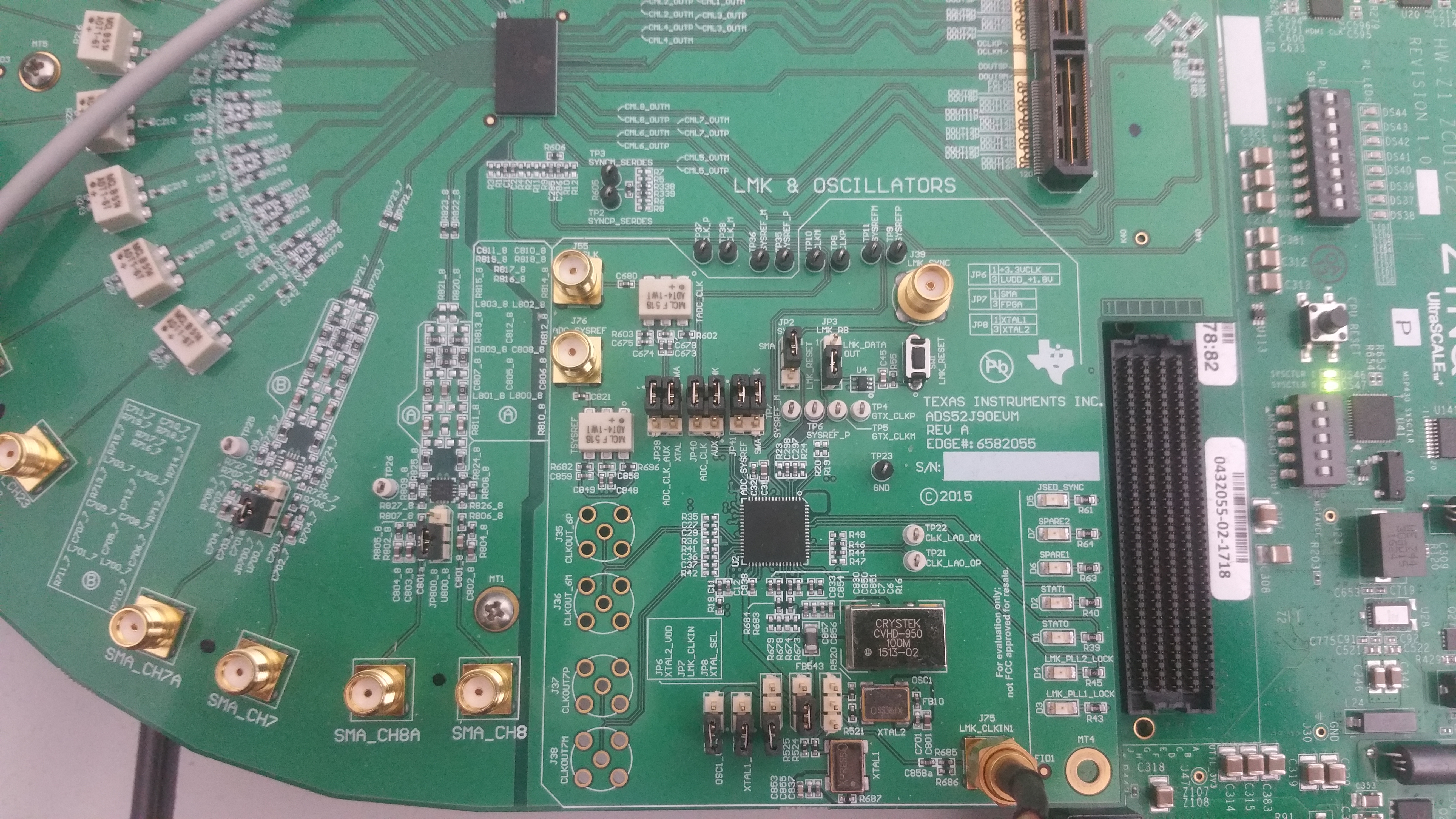
I am using TI's High speed ADC board ADS52J90EVM. I am using Xilinx Zynq Ultrascale+ board to read ADC samples But before this i wanted to see if the adc is configured properly and is giving out all the required signals. Therefore i have connected ILA debug core to the ports of ADC.

I can see Sysref Signal periodically repeating, Ref Clk is also working. but the FPGA CLK signal is low all the time.

I am using the quick start jesd configuration. (please see the attached file)

Could you tell me what could be the issue ?

Thanks alot for assistance.
Best Regards
RizwanADS52J90_16ch_SINE_4L_12x_12b_GBLCLKDIV1_FSDIV3_SYSREFDIV24_20x.cfg

  • Hello Rizwan,

    A quick question, have you checked the configuration with the TSW14J56EVM?
    I will check the configuration file and see if there are any issues and will get back to you.
  • Hello Praveen 

    Thanks alot for your response. 

    I dont have TSW14J56EVM capture card. i am using ZCU102 xilinx board to read samples.

    My plan is to check first if the ADC signals are coming as per the JESD configuration. and then i will connect these signals with the JESD ip core in Vivado. 

    The Vivado IP core accepts two clocks

    1- Ref Clk

    2- Glb Clk

    ADS52j90 EVM also gives two clock 

    1- FPGA_GTXCLK P/M 

    2. FPGA CLK  P/M

    I am connecting FPGA_GTXCLK  to the Ref CLk  and FPGA Clk to GLB clk. 

    Thats why it was important for me to see if the both clocks are functional .

    Do you think i am going in the right direction ? 

    Best Regards

    Rizwan 

  • Hello Praveen

    Do you have any updates on it ?


    Best Regards
    Rizwan
  • Hello Rizwan,

    Can you provide the clock configuration jumper settings on the EVM?
    A snapshot of the EVM showing the jumper configurations on the bottom right section will also do.
    What is the clock frequency that you provide on J75?

    As I mentioned in my other post, I am not familiar with the Vivado IP core.
    Let me check with the software team regarding your question on where to connect the GTX and FPGA clk on the Vivado and will get back as soon as I have a response.
  • Hi Praveen 

    Thanks alot parveen for your reply. I have attached the photo of my EVM. 

    Currently i am supplying 120 Mghz at J75

    I have checked some Vivado reference designs, and in those designs clock signals are connected as i described above. That's Why i wanted to know why i am not able to see the clock ( FPGA_CLK) on evm. this clock is also observableon test point TP22 and TP21. 

    Thanks for assistance :)

  • Hi Parveen 

    So i dig a little deeper in to it. 

    FPGA CLK  ( on ADC EVM ) is coming from DCLKOUT8p ( from LMK04826 ). so LMK04826  is generating all the clocks for the ADCs. i.e. GTX clk, sysref etc.  

    I checked the datasheet of LMK04826 to confirm if i am setting the register for the DCLKOUT8p  correctly. the register address is 120x and its value is 0x04 ( clock divided by 4 ) . it means that the register setting is also correct. 

    Could you please comment on it, where could be the problem with this clock. ? 

    Best Regards

    Rizwan 

  • Hi Rizwan,

    I checked the LMK register configuration and the LMK is set up to generate the FPGA clock but the clock output buffer is powered down (register address 0x126).
    You may want to enable the clock buffer.