This thread has been locked.

If you have a related question, please click the "Ask a related question" button in the top right corner. The newly created question will be automatically linked to this question.

DAC37J84: Phase noise under low temperature

Part Number: DAC37J84
Other Parts Discussed in Thread: LMK04828, DAC38J84

Hi,

I would like to ask you a question and support about phase noise of DAC37J84.

According to my customer, the phase noise is somtimes getting worse when temperature is under low.

The spectrum is as below. ("NG" is worse case.)

1) normal
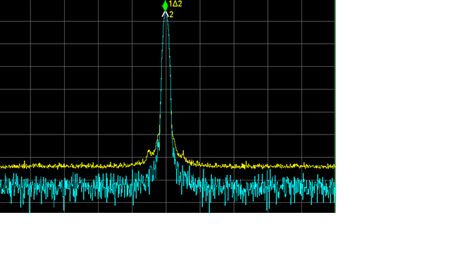
2) NG
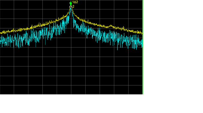
This phenomenon is not always happened under low temperature.

And, the customer uses multiple DAC37J84s on the board and the phenomenon does not happen at all devices.

The configuration of the circuit is "LMK04828+DAC37J84".

I suppose the most influential factor to get phase noise worse is "clock" which is applied to DAC37J84.

Could you advise me any other possibilities to getting worse, for example, power noise, borad layout(signal pattern of clock), etc?

Thank you for your support.

Best Regards,

  • Hello Takumi-san,

    I would check to see if the phase noise of the LMK04828 clock is also being impact at cold temperature.Please ask the customer to measure the LMK04828 clock to the DACCLK input of the DAC38J84. I would like to make sure the clock source is clean before further move into DAC38J84 debug.

    Typically, the DAC phase noise performance is limited by the clock source and/or the clock drive (internal to the DAC) power supply quality

    at this point, if we are safe to rule out the LMK04828 quality, then we can check:

    1. if the on-chip PLL is used, please check if the PLL is still within the optimal lock range. You can read back the PLL loop filter voltage through register config 0x0031. We may need to adjust the PLL voltage (i.e. VDDPLL18) to slightly higher of the specification and check if it fixes the problem. (see below for ATEST method). 

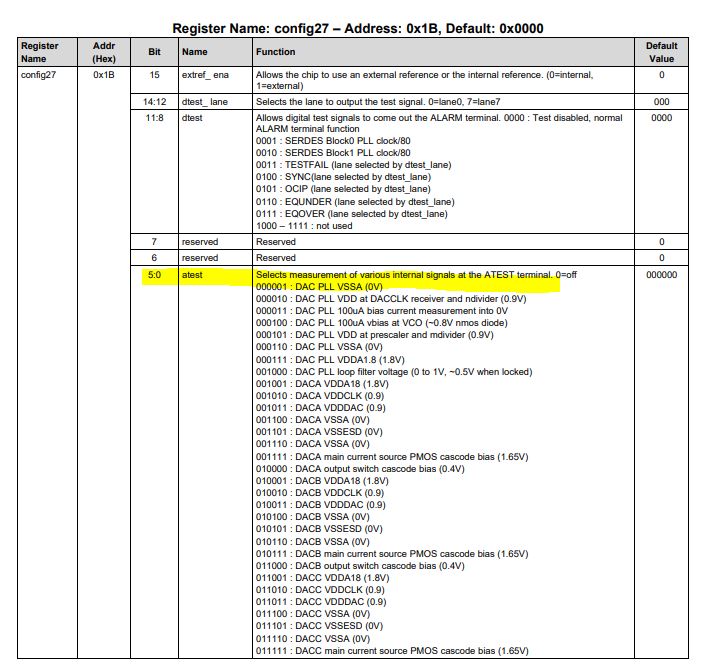
    2. Use the ATEST pin on the device, program register 0x001B to walk through some of the critical ATEST nodes. Typically, the VDDCLK voltage are sensitive to LDO/DC/DC power supply noise. Perhaps at cold temperature there are increase in noise and also drop in the voltage level. 

    If the LDO powering the VDDCLK has noise at cold temperature, then the noise will modulate onto the power supply of the clock buffers internal, and hence modulating onto the output.

    To ensure the voltage level at the device internal nodes are correct, please program 0x0027 to check all the nodes to make sure they are within the specification.

    -Kang

  • Hi Kang-san,

    Thank you so much for your kind reply!

    I understood well.

    But let me confirm one point as below.

    I do not understand well what you point ".......please program 0x0027 to check all the nodes...".

    What is "0x0027" register? I suppose this is the register reserved..

    Does this mean "Config27(0x1B)" ??

    I would appreciate your support very much.

    Best Regards,

  • Hi Kang-san,

    Sorry, let me please confirm one more point as below?

    About your advice "We may need to adjust the PLL voltage (i.e. VDDPLL18) to slightly higher of the specification...",

    "VDDPLL18" means "VDDAPLL18", correct?

    and about  "slightly higher of the specification", what voltage do you intend?

    Thank you for your support!

    Best Regards,

  • Tamkumi-san,

    regarding your question:

    Takumi Suzuki1 said:

    I do not understand well what you point ".......please program 0x0027 to check all the nodes...".

    What is "0x0027" register? I suppose this is the register reserved..

    I was referring to the ATEST programming. Basically, the engineer may use a voltmeter with respective to the ground to measure the ATEST pin (K9 pin of the device) and measure the internal nodes. The internal nodes are programmed by the ATEST registers in the 0x001b (config27) register. I apologize I made a typo on the ATEST register. 

    I have pasted the register information below:

  • Takumi-san,

    The reason that I asked the customer to raise the voltage slightly is because there may be PCB resistance and power supply filter resistance at the power supply node (LDO or DC/DC). With the current drawn, the resistance created voltage drop and may not provide the right level at the operation. I ask the customer to raise the voltage slightly such that when the chip is turned on, the voltage level falls within the specification. The customer needs to be careful since before the chip is turned on (without current drawn), the voltage may be higher since there are no voltage drop. Therefore, the power supply may still need to be within the higher range of the specification, even with the chip turned off.

    The ATEST procedure will help identify if there are significant voltage drop at the problematic temperatures. Perhaps the LDO need to be adjusted at such temperature.

    -Kang
  • Kang-san,

    Thank you for your reply !

    No problem, thank you so much for your support.

    Best Regards,

  • Kang-san,
    Thank you very much for your explanation, I understood well !
    Best Regards,
  • Kang-san,

    I am working with Takumi, and I would like to update the customer's status.

    Out customer tried to change the output voltage of 0.9V- LDO which is supplied to VDDCLK09, VDDDAC09 and VDDT09 at Ta = -20dec C.
    When the LDO was lowered to 0.8 V, a tendency to decrease the noise floor was recognized, and further lowering to 0.760 V lowered the noise to the same level as at room temperature.
    Also, they tried raising the voltage of 0.9 V - LDO to 0.95 V, but there was no improvement in the noise floor.
    This 0.9V-LDO is also supplied to another DAC, and it was normal for the noise floor at any temperature.
    The symptoms are different even though the same power supply is supplied.

    Is there anything you can understand from this?

    Best regards,
    Toshi
  • Toshi-san,

    We may need to review their configuration sequence. Please let us know if they can share

    If the DAC is in external clock mode, then I do not see the reason that lowering the voltage will help lower the noise floor.

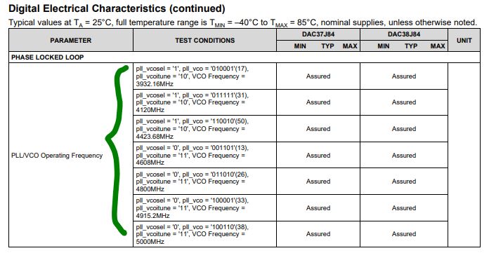
    I suspect the customer is using the on-chip PLL/VCO circuit, and the tuning of the VCO circuit may not be set up correctly.

    Please double check (if PLL/VCO circuits are used) for their exact PLL_VCO_SEL, PLL_VCO, PLLVCOITUNE per their VCO configuration.

    If they are indeed correct, we may need to adjust their PLL_VCO code to see if problem is fixed. We may need to ask the customer for some units for FA afterwards.

  • Kang-san,

    thanks for your advice.

    In their application there are tow types of boards that use PLLs and boards that are not using them. The phenomenon that the noise floor rises at low temperature are happening in either case.

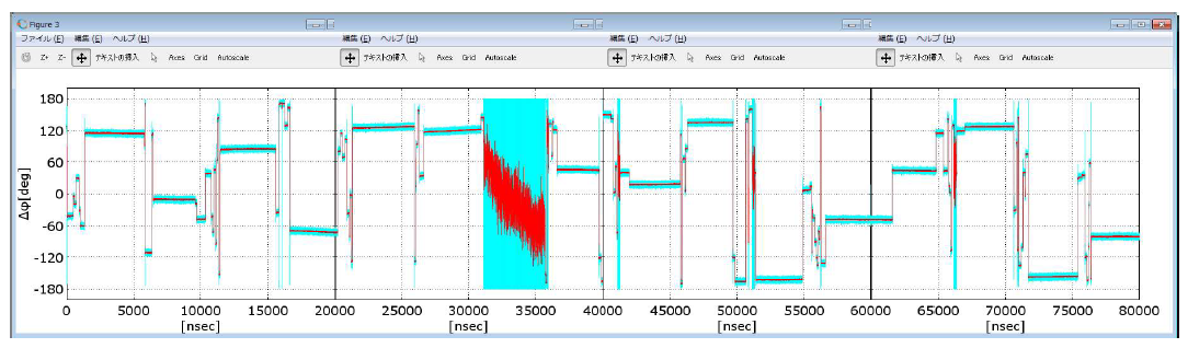
    When this phenomenon is occurring, the time interval varies depending on conditions, but a phase change occurs at intervals of about 4 us - 5 us.

    The following capture screen monitors the phase change when single tone is output.

    Their setting is being reviewed again.

    I hope this information will help in the analysis.

    Best regards,
    Toshi

  • Toshi-san,

    Could you please advise the expected phase change in normal operating condition? Should the curve be a straight slope line from 0degree to 360degree?

    The fact that phase is changing drastically seem to indicate some of the bits may be having error. Could the customer advise if they are using NCO in the DAC? Could they please try to use "NCO sync" and "Mixer sync" to trigger a reset to the NCO accumulator to see if the NCO is miscounting the sine/cosine wave internal to the digital mixer? If there are miscounts of sine/cosine wave in the digital mixer, the output phase noise could also be degraded.

    I suspect the temperature drop must have caused some power supply node (especially DVDD) to sag (drop in voltage) temporarily. This sudden drop in voltage causes bit error in the data path and caused drop in phase noise performance.

    -Kang
  • Kang-san,
    The expected phase change in normal operating condition is a straight line, like 0-degree and this has been verified at room temperature.
    The CW signal of the output is generated by the data written in the DAC, and it is not generated by the NCO.
    From the above circumstances, should I check DVDD?

    Best regards,
    Toshi
  • Kang-san,

    My customer plans to check the digital power supply.

    By the way, if the steady state is 0 °, even if a bit error occurs, I think that it will be temporarily shifted from the steady state. It seems that the data is stable with the phase shifted for a certain period after shifting the phase to a certain place, so it seems that it can not be explained with only bit error alone.
    As a phenomenon, it seems that it will not become such a waveform of the phase change unless the clock etc. deviates or the FIFO pointer etc. is shifted, so it may be necessary to investigate whether there is any other cause.

    Would you give me some advice to explore the cause a little more?

    Best regards,
    Toshi
  • Toshi-san,

    I think DVDD is a good start. Please probe as close to the device to include DC resistance throughout the path.

    Other ways to probe deep into the matter includes reading back the status alarm bits between config100 to config108. We need to understand if there are other alarms/error happening. Please ask the customer to first clear the alarm (by writing all zeros) and then perform read back on the latest status.

    I also wonder that the phase shift are quite abrupt may be due to the JESD204B link breaking. Could you ask the customer to probe the LVDS SYNC line to see if it is toggling the same fashion as the phase change?

    -Kang