This thread has been locked.

If you have a related question, please click the "Ask a related question" button in the top right corner. The newly created question will be automatically linked to this question.

ADS54J60: How is interleave correction processing done?

Part Number: ADS54J60
Other Parts Discussed in Thread: , LMK04828

Q1.

[datasheet] 8.5.2.4.8

If 7 bits (CTRL NYQUIST) of Register 4Eh is default = 0 (disabled), Interleaving correction in the block diagram of 8.2 does not processing anything?

I want to know specifically the processing procedure when CTRL NYQUIST is enabled.

Q2.

[datasheet] 8.2

Please tell me about the processing of Interleaving correction in the block diagram of 8.2.

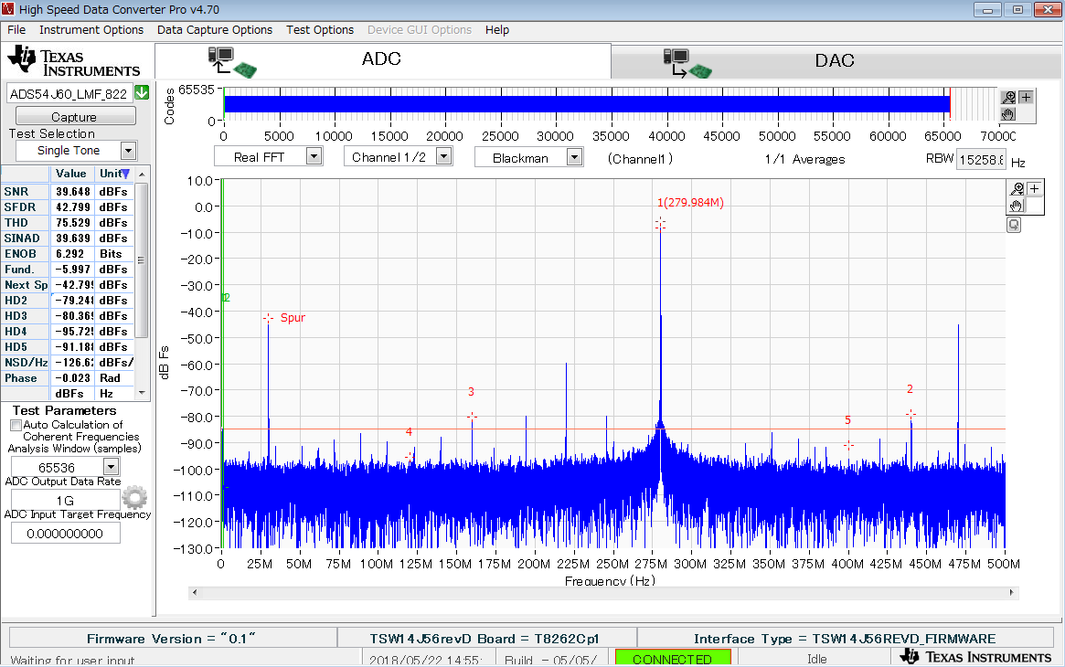
Also, What is the effect of Interleave correction in undersampling do you think ? 

(I am concerned about SFDR being degraded by Interleave correction)

  • Witlab,

    Q1:

    Nyquist zone CTRL enables additional interleaving correction for analog mismatch. Nyquist zone information tells the interleaving correction the  proper analog input frequency range.


    Q2:

    The ADS54j60 includes several different internal correction blocks to correct interleaving spurs due to timing, gain, offset and bandwidth mismatch of the  individual ADCs. Figure 21 in the data sheet shows the IL spurs (worst one) across input frequency.

    More info can be found in attached document.

    Regards,

    Jim

    5554.ADC Basics.pdf

  • Jim-san

    Thank you for your reply.

    I have a problem with Interleaving spur of undersampling.

    In ADS54J60 data sheet, SFDR_IL = 90 dBc at fin = 720 MHz, Ain = - 6 dBFS, at ADC sampling rate = 1.0 GSPS (2nd Nyquist zone).

    However, when we measured under the same condition written in the data sheet, SFDR_IL is only about 42 dBc obtained.

    Please let me know if you know the cause, such as the measurement conditions and whether Nyquist zone CTRL is valid or not.

    <Measurement condition>

    ・We used ADC Evaluation board(ADS54J60EVM)

    ・ADC sampling rate = 1.0 GSPS

    * External LMK04828 Clock (Clock Distribution Mode) is used. (in ADS54J60EVM User's guide 5.1.2)

    1.0 GHz for clock is supplied to the J6 connector from the signal generator.

    ・fin = 720MHz, Ain = -6dBFS(differential input)

    * We constructed differential input configuration with reference to ADS54J60EVM User's guide 5.2.1.

  • ADS54J60_LMF_8224_2NQ.cfgWitlab,

    Try using this attached file for the ADC. There is a register that has to be set to match the Nyquist zone the analog input is at.

    0x680042 0x01 //2nd Nyquist zone select
    0x68004E 0x80 //nyquist enable

    Regards,

    Jim