This thread has been locked.

If you have a related question, please click the "Ask a related question" button in the top right corner. The newly created question will be automatically linked to this question.

ADC12DJ3200: ADC12DJ3200 interfacing with Xilinx kintex Ultrascale (KCU105)

Part Number: ADC12DJ3200

HI,

I am using the following setup.

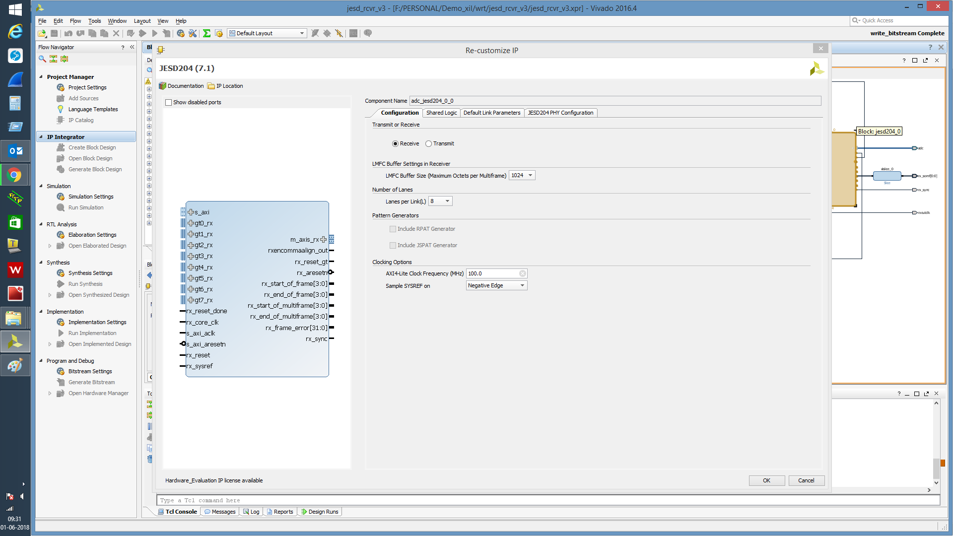
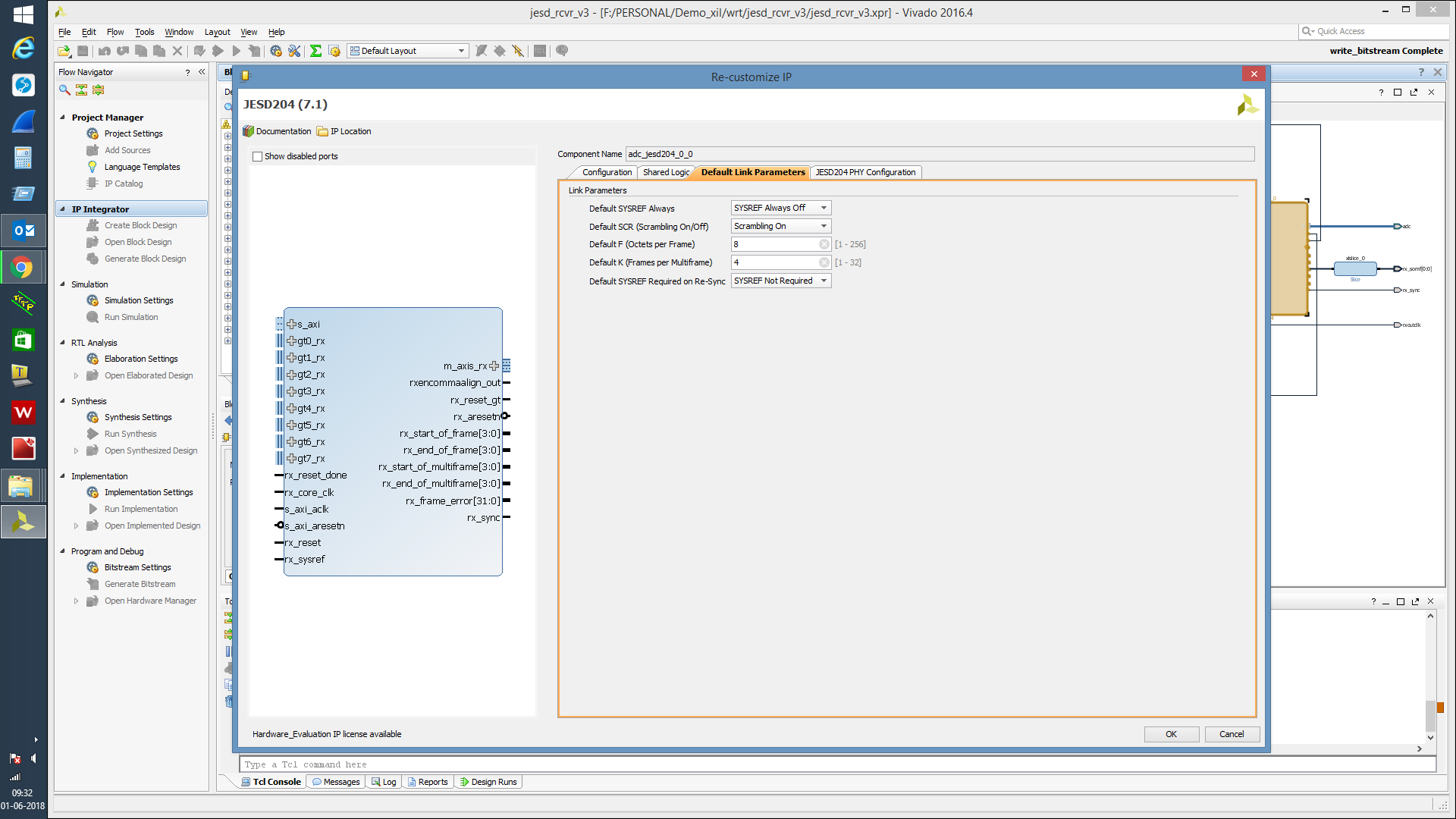
ADC12DJ3200EVM which is interfaced with the xilinx KCU105 Evaluation board. 

There is an reference design and document provided i am using it (ADC12DJ3200 reference Design 6Gbps.zip & KCU105 ADC12DJxx00 JESD Reference Design User Guide.pdf).

I am setting JESD test mode to ramp test and enabling the commands through the ADC12DJXX000 GUI as per the below screen shot.

We are getting the ADC data from the converter but as per the document all the 8 lane data needs to be same but we are getting 4 lane data as same and another 4 lane different data.

here by i have attaching the screen shot for your reference.
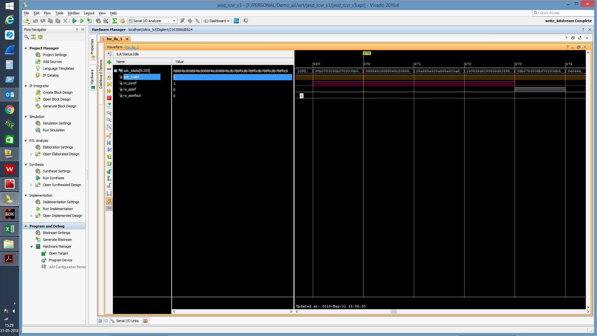
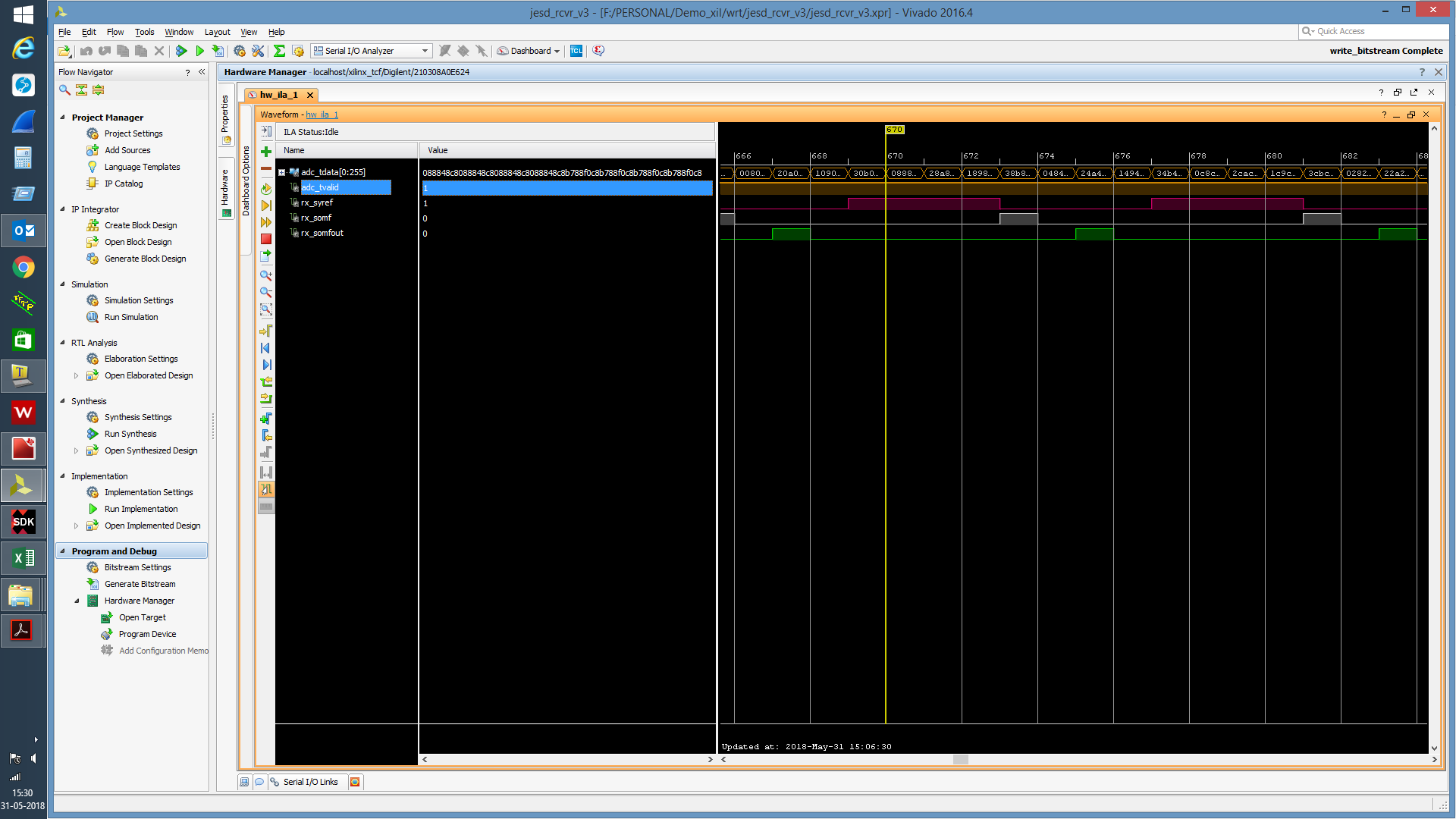
kindly please help.

Note:

ADC sampling period is set to 3.2 GSPS and Lane rate at the xilinx IP is set to 12.5 Gb/s.

Regards,

Rajesh.

  • Hi Rajesh
    I am reviewing your question and will send a response later today.
    Best regards,
    Jim B
  • Hi Rajesh

    For JMODE0 and Ramp test pattern mode, all 8 lanes will have the same information. The data in each lane will be a sequence of increasing octet values that starts at 00 and increases to FF then goes to 00 and repeats the same progression.

    There may be an issue with the published reference design you are using that isn't compatible with the production version of ADC12DJ3200EVM that you have. This will cause the data in some lanes to be incorrect.

    Please try the changes mentioned in this earlier thread and let us know if that resolves the issue or not.

    https://e2e.ti.com/support/data_converters/high_speed_data_converters/f/68/p/670226/2477154#2477154

    Best regards,

    Jim B

  • Hi Jim,

    Thanks for your immediate support.

    I would like to give additional info on the EVM, we have received the EVM (ADC12DJ3200EVM REV A (s/n:4730300008))from the bangalore for evaluation.It might be same as the Mr.Manjunath used.

    we have also got one shipped by the TI with Altera Arria but we are not using this module since we wanted to interface with xilinx only, ADC12DJ3200EVM REV A (s/n:4963000047). i will also check with this EVM too.

    *******************************************************************

    After some digging we determined that the ADC12DJ3200EVM files created for the KCU105 were based on a pre-production version of the ADC EVM. Some changes to the EVM data lane polarities cause problems when using the production EVM. The 2 files contained in the following .zip file will resolve the issues you are having:

    /cfs-file/__key/communityserver-discussions-components-files/73/3817.KCU105_5F00_ADC12DJ3200EVM_5F00_Update.zip

    The .dll file should be copied into this folder location: C:\Program Files (x86)\Texas Instruments\High Speed Data Converter Pro\KCU105 Details

    The .ini file should be copied into this folder location: C:\Program Files (x86)\Texas Instruments\High Speed Data Converter Pro\KCU105 Details\ADC files

    ********************************************************************

    Currently i am not using HSDC Pro for checking the adc data, i need to first see the data from the adc on FPGA end reliably since our application needs to take adc data and do some processing.

    (i am downloading the HSDC Pro). even when it is not used we need these dll for operation to monitor on FPGA.

    additional note:

    please find the setting used in Xilinx JESD IP core as screen shot.

    Regards,

    Rajesh

  • Hi Rajesh

    The change between the pre-production EVM used for the original reference design development, and the production Rev. A EVMs that you are using is as follows:

    On the Rev A EVMs, the ADC lanes DB0, DB1, DB2 and DB3 are inverted in polarity to ease routing on the board and improve signal integrity. The corresponding FMC connector signal names are as follows:

    • FMC_HPC_DP4_M2C
    • FMC_HPC_DP5_M2C
    • FMC_HPC_DP6_M2C
    • FMC_HPC_DP7_M2C

    To see the correct data you will need to invert the polarity of those lanes before they are input to the JESD204B receive IP.

    The files referenced in the earlier thread accomplish this inversion using information from the following .ini file commands:

    • Invert Serdes Data = 240 (this inverts the upper 4 lanes)
    • Enable Individual Lane Inversion = 1

    Best regards,

    Jim B