This thread has been locked.

If you have a related question, please click the "Ask a related question" button in the top right corner. The newly created question will be automatically linked to this question.

ADS1299: ADS1299: Testing bias / Right-leg drive

Part Number: ADS1299

I'm testing acquisition of EEG data with ADS. I have included the chip on a custom PCB with the necessary power supply (from battery) and signal conditioning for the input signals. A raspberry pi (RPi) is used to acquire samples from the amplifier through SPI.

To test data acquisition, I have two GPIO pins on the RPi generate delayed 10Hz and 7Hz square waves (between GND and 3.3V), which are then attenuated by voltage divider network by 100 before feeding into IN1P and IN2P of the amplifier. GND is fed into SRB1 of ADS, and the ADS operate in referential montage with respect to SRB1. The VSSA and VDDA for ADS are -2.5 and +2.5V. This works as expected and I acquire the different 10Hz and 7Hz waveforms (described by box 1 in the Figure 1 below).

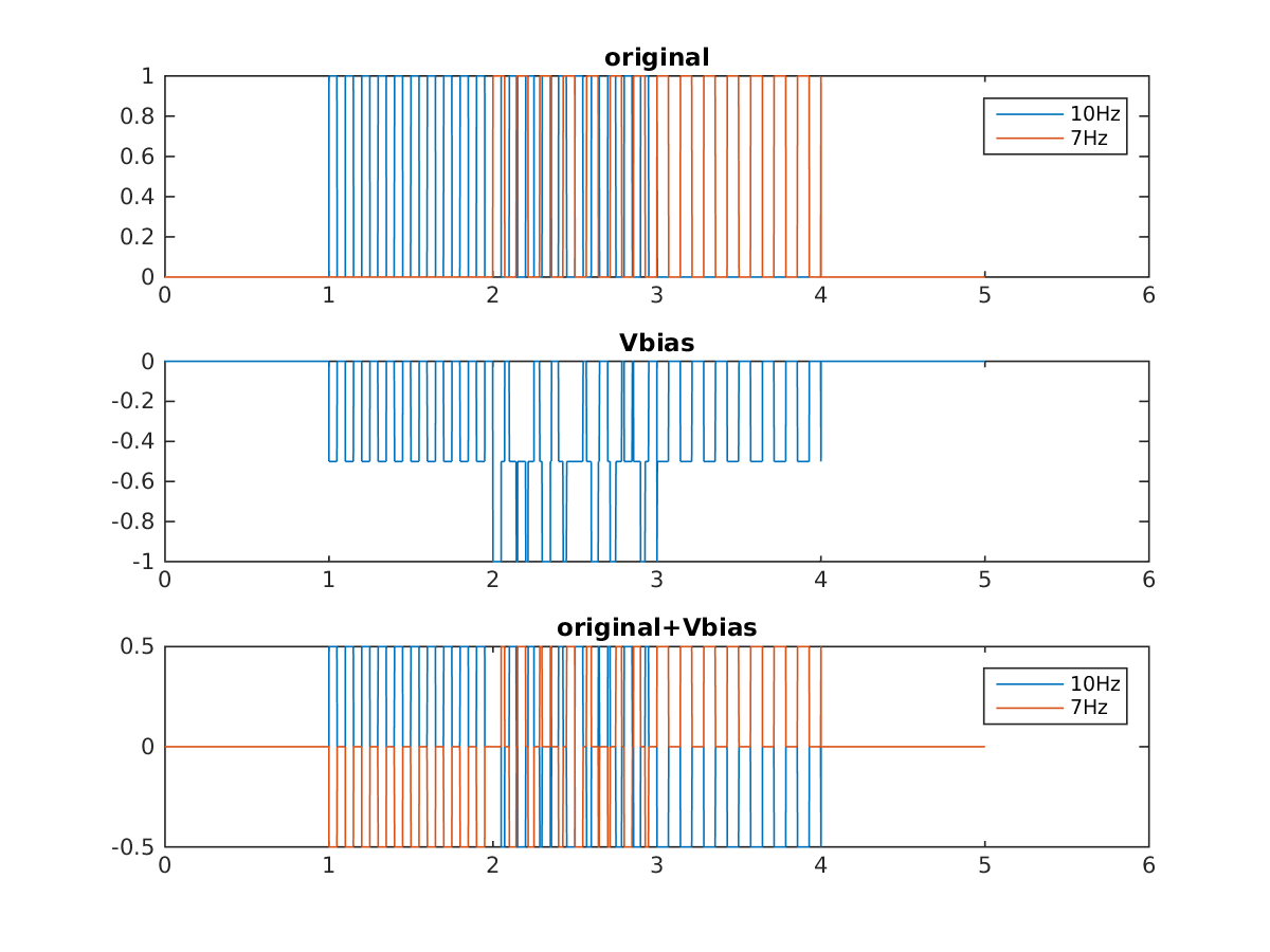
I then want to test the right-leg drive by the bias amplifier. My test setup is indicated in box 2 in the Figure 1: the attenuated square waves are buffered and summed with Vbias before entering ADS. I configured the bias amplifier to take the average of the measured signals. This resulted in something similar to that in Figure 2 (Vbias calculated as the average of the input signals):

On the scope the output (original+bias in the figure) has ripples due to the Rf-Cf feedback of the bias amplifier. While the results are exactly what I expected, I am not sure if my test setup models RLD correctly -- in the original+Vbias plot, during the time period where the 10Hz and 7Hz overlap, the frequency information is lost distorted.

The purpose of RLD is to enhance common-mode rejection...an alternative I could think of is to add a small common mode Vcm to V1 and V2 (box 3 in Figure 1). But it would still not be able to preserve the 10Hz and 7Hz information in the resulting signals.

I have read the SBAA188 application report on right-leg drive, in its test setup in Figure 7, it applies the same signal to both input channels (one through RC-network, the other no RC-network). But this does not address the distortion of the measured signals by the bias signal. Am I understanding this correctly? What is the correct way to model the effects of RLD?

  • Hello Allen,

    Thank you for your post and welcome to our forum!

    I'm a little confused by what the Matlab plots are referring to - please try to clarify this for me:

    1. "Original" - is this showing the output of Channel 1 and Channel 2 without VBIAS? The input signal in this case is a 0 - 300mV square wave (i.e. 300 mVpp centered around 150 mV) connected to INxP while SRB1 is used to connect INxN to ground. What is the gain of the PGA?
    2. "VBIAS" - is this measured or calculated? You can actually measure the output of the BIAS amplifier directly through one of the channels. Set the appropriate channel to MUXn[2:0] = 010 and set CONFIG3[4] = 1. BIASOUT will have to be connected to BIASIN on your board.
    3. "Original + VBIAS" - this is the measured output of Channel 1 and Channel 2 with the circuit (2) configuration? In theory, if only V1 or V2 was selected for BIAS_SENS, then I believe this should do what you expect and cancel the buffered V1 or V2 signals through the 100k summing junction. However, the BIAS output will contain both signals in the circuit you have drawn, so I believe 7 Hz will show up on Channel 1 and 10 Hz will show up on Channel 2. Is that your expectation?

    Also, remember that you are driving square waves into the device, which are comprised of many higher frequency components than the fundamental 7 Hz or 10 Hz. The BIAS amplifier closed-loop bandwidth is currently set to ~133 Hz, so the common-mode cancellation signal at the BIAS amplifier output will not contain those higher frequency components and you will not be able to reject them. Can you substitute V1 and V2 with 300 mVpp amplitude sine waves from a function generator?

    A couple comments on the schematic drawing:

    1. V2 should be connected between the 100k and 1.2k resistors, just like V1, correct?
    2. You are missing the PGA between INxP and the 220k BIAS sense resistors. Remember that input signal will see gain before the BIAS amplifier.

    Best Regards,

  • Thanks for the quick reply. Sorry for the inaccurate plots, the Matlab plots were to demonstrate the shape of the waveforms. The clarifications:

    1. "Original" is showing the output of Channel 1 and Channel 2 without VBIAS summed. The configuration is as you described, gain of the PGA is 24. The square wave was generated in the 0-3.3V, then attenuated to 0 - ~40mV by the voltage divider before entering the PGA.

    2. "VBIAS" - this is calculated, to describe the output of the BIAS amplifier. I measured the shape and frequency on the actual BIASOUT pin with the scope and it agrees with this calculation.

    3. "Original+VBIAS" - this is the expected output of Channel 1 and Channel 2 with the circuit (2) configuration. My expectation is exactly as you describe, i.e. "the BIAS output will contain both signals in the circuit you have drawn, so I believe 7 Hz will show up on Channel 1 and 10 Hz will show up on Channel 2"

    So here lies my trouble in understanding RLD -- say both Channel 1 and Channel 2 has frequency components [f1, f2, ...fn], all within the closed-loop bandwidth,  with each frequency component containing different amount of power for different channels. If I take their average and apply inverse of that to cancel the common mode, that would add Channel 2's frequencies onto Channel 1, and vice versa. This then distorts the actual frequency contents in both channels. Is my understanding correct, or am I not testing this correctly?

    You are right that V2 should be connected between the 100K and 1.2K resistor, just like V1...silly mistake on my part. And you are right, I omitted the PGA between the INxP and 220K BIAS sense resistor...I was taking the gain for granted.

  • Hi Allen,

    I believe that Ryan and I's colleague Brian explained RLD drive well in this post: e2e.ti.com/.../604038

    Quote below:

    "Let me just begin by explaining the purpose of RLD. In a typical ECG system, you might have 3 or 4 electrodes. One of those electrodes is called "RL". If you read the definitions of the ECG leads, you'll notice this electrode is not actually used to form any leads. The RL electrode serves two purposes:

    1) Bias the patient. If the electrodes are all DC coupled to the patient, there needs to be some way of biasing the patient such that the electrode common-mode voltage is within the rails of the AFE. The average RL voltage will typically be (vdd + vss)/2. This voltage is applied to the patient putting his/her dc bias right in the middle of the AFE's common-mode range.
    2) Reject common-mode signals. There is so much common-mode interference in the environment mostly from 50/60Hz mains frequency junk (i.e. florescent lights, fans, motors, etc.). This stuff easily couples on to the patient capactively. From an electrical engineering perspective, this does not initially sound like a problem, because the AFE can have very good CMRR. However, the impedance of the connections between the electrodes and the patients can be vastly different and cannot be controlled easily. This causes massive impedance mismatch between the inputs. So bad, in fact, that it does not matter how much CMRR your AFE has since the CMRR of the electrodes is terrible. To get around this, you sense the electrode common-mode voltage using the AFE, and invert that signal and apply it to the patient via the RL electrode. This does a good job of getting rid of most of the interference."

    Hope this helps!
  • I have read this post and other papers on RLD and understand and agree with the theory and what you said. I am having problem testing and applying this, specifically in the situation I outlined where feeding back the common-mode signals result in introducing channel 1's frequencies into channel 2, and vice versa. I'm wondering if you could comment on any problems with my test setup, and on how I can tell if RLD is indeed working in a given setup.

  • Allen,

    I apologize for not providing the best guidance here, but I will do my best. Ryan will be back in the office next week.

    Have you had a chance to substitute V1 and V2 with a 300 mVpp amplitude sine wave from a function generator as he suggested?

    I believe that your understanding is accurate and that channel 1's frequency will be introduced to channel 2 & vice versa in this test setup. However the purpose of the RLD is to remove the noise that is common to both channels i.e. the lights. Purposefully introducing different frequency square waves on both channels will certainly introduce the opposite channels frequencies into the other as the average is taken and inversely applied to both channels through the RLD.

    Using two frequencies that are easier to distinguish may help your analysis and make it easier to understand your matlab plots. Perhaps 5Hz & 10Hz or 10Hz & 20Hz as opposed to 7Hz & 10Hz. Do you agree?
  • Hi Allen,

    Hope all is well.

    Are you still working on this, or are you comfortable with how BIAS is working on the ADS1299?

    The way you modeled the initial circuit is similar to how the BIAS amplifier output actually affects the signals on the body. The common-mode cancellation signal and the biopotential signals sum together through the impedances of the body and the electrode-skin interface. What you are assuming, however, is that all of these impedances are equal, and that the common-mode signal will add equally to the signal of interest. This will not likely be the case.

    If your goal is simply to validate the BIAS amplifier output without a scope, you can configure the MUX to route BIASOUT into one of your other channels (i.e. CH3). Then, configure that channel for BIAS output measurement, which will automatically create a differential measurement between BIASOUT and BIASREF. Remember that the PGA gain will amplify that differential signal. Please see section 9.3.2.4.2 for details on the MUX configuration and the required register settings.


    Best Regards,
  • Hi Ryan,

    I still have not resolved the issue...I replaced the square waves with sine waves, and the same problem persists -- the bias signal formed from averaging individual channels contains frequency components of all the input channels and therefore each recorded channel gets injected with the other channels' frequency components. It is not clear to me how impedance mismatch in each channel can solve this. Although if both channels are contaminated with common mode noise, say 60Hz power line, the 60Hz noise will be subtracted from the input channels.

    So far, my conclusion about the RLD is that it indeed removes common mode noise, but mixes the differential mode...I'm thinking one possible solution is to set the bandwidth of the bias amplifier to below the EEG signals of interest (say below 1Hz). But this approach would not be able to filter out high frequency common mode noise (which may not matter too much since EEG bandwidth is limited to below 50Hz). Any suggestions?

  • Hi Allen,

    I think what we're forgetting is that the signal content contained in the bias amplifier output will be common to all other measurement electrodes and is only cancelled when the channel makes the differential measurement: INxP - INxN. Right now, you are measuring each positive channel input (INxP) with respect to ground. Therefore, the common-mode signal from the bias amplifier will also show up on each channel's output. However, this should be cancelled whenever the differential measurement is made - even if you do this digitally in some post-processing (i.e. CH1 - CH2). Typically, this is done in analog, where the INxP input is the measured electrode and INxN is a common reference electrode. This reference electrode would contain all of the same common-mode signals injected from the bias amplifier. That was the original intention behind the SRB1 pin.

    Let me know if this makes sense.
  • Ahhh ok, this makes sense. So I really should have a virtual ground and sum the bias output there as well in my test setup. Is this correct?
  • So like this: