A related question is a question created from another question. When the related question is created, it will be automatically linked to the original question.
If you have a related question, please click the "Ask a related question" button in the top right corner. The newly created question will be automatically linked to this question.
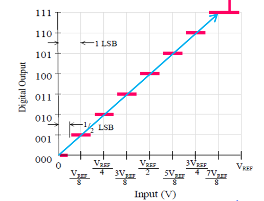
An ideal transfer function for a ADC has a transition point at LSB/2 voltage, the steps are designed to have transitions such that the midpoint of each step corresponds to the point on this ideal line. Here is an example:
Assume an ideal 3 bit ADC with bipolar input range = -4V to 4V:
FSR = 4-(-4) = 8V
ADC codes = 2^3 = 8
LSB size = 1V
LSB/2 = 0.5V
If we plot the transfer curve for the above ADC, the transition points will be as per table below.
As you can notice, at NFS the region is (NFS+0.5LSB) and at PFS this is (PFS-1.5LSB)
Code
Transition Point (V)
Voltage Range (V)
-4
-4
-4V to -3.5V
-3
-3.5
-3.5V to -2.5V
-2
-2.5
-2.5V to -1.5V
-1
-1.5
-1.5V to -0.5V
0
-0.5
-0.5V to +0.5V
1
0.5
+0.5V to +1.5V
2
1.5
+1.5V to +2.5V
3
2.5
+2.5V to +4V
Another example for unipolar input ADC shown as below, the first transition happens at 1/2 LSB, and the last transition happens at Vref-1.5LSB (Full scale range is Vref).
Hopefully this is helpful for you to understand, thanks.