This thread has been locked.

If you have a related question, please click the "Ask a related question" button in the top right corner. The newly created question will be automatically linked to this question.

ADS1258: I have two questions about ADC IC (ADS1258MPHPTEP).

Part Number: ADS1258


 have two questions about ADC IC (ADS1258MPHPTEP).

* Designed contents are as follows.

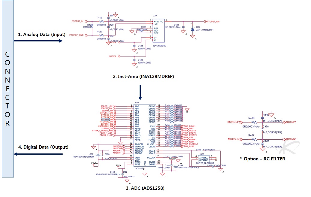
 - 1.Analog Data (Input) -> 2.Inst-Amp (INA129MDREP) -> 3.ADC (ADS1258MPHPTEP) -> 4.Digital Data(Output)

* Inquiry 1. Offset occurs

  - An offset of about 1.006 % occurs when the input analog data is compared with the output digital data.

   (ex: Input: 1V -> Output: 1.006V, Input : 2V -> Output: 2.012V)

 - I want to know why there is an offset and if there is a design problem.


* Inquiry 2. Remove Offset

  - When designing the R-C filter on the outside and designing the feed-back of the MUX data by "ADC 43-44 pin-> R-C filter-> 41/42 pin"

   The offset that occurred in Inquiry 1 has been removed.

  - I want to know why the offset has been removed.

      @ RC Filter Applied value: 130 Ohm, 100pF, Cut-Off Frequency: 6.18MHz


  • Hi Choe,

    Welcome to the TI E2E Forums!

    1) Regarding your first inquiry about the 1.006% offset..

    This may be a combination of offset and gain error. Generally, an offset error is constant for all input voltages. The best way to determine the offset is to measure the result with a 0V input.

    Gain errors, on the other hand, scale with the input signal. In your example 1V -> 1.006V and 2V -> 2.012V looks more like a 0.6% gain error. The ADS1258 is specified to to have a typical gain error of 0.1 % or a maximum gain error of 0.5%, so this is a bit higher than normal for the ADS1258. However, you may have some additional gain error coming from the INA, so it is quite possible that the combined gain error is 0.6%.

    One way you might be able to resolve this error is to perform offset and gain error calibration. This involves measuring the offset and gain error and then correcting for them when performing software calculations. Since offset and gain error have some static components (constant errors that do not change over time and temperature), calibration is able to greater reduce the system's overall error. For more information on this topic see : training.ti.com/ti-precision-labs-adcs-offset-and-gain-calibration


    2) For your second inquiry, I can't say for certain what is happening since this would depend on a lot of factors, including which ADC inputs you were measuring and the signal source's output impedance. The introduction of series resistors in the input path can result in small voltage drops across these resistors. These voltage drops can be the result of input bias currents and R or C component mismatches. Since you have small resistor values I wouldn't expect that to be an issue; however, do pay attention to the matching of C379 and C380, as mismatches between these components can convert common-mode signals into offsets. To avoid this, I would recommend making C379 and C380 10x times smaller than C378 to reduce this effect.


    One other thing to be careful with is how you connect the analog and digital grounds in your circuit. The ADS1258's analog and digtial grounds needs to be shorted at the device. In you schematic these grounds are separated and no connection between these grounds is shown. This can often lead to additional offset error, as well as many other issues; therefore, I would recommend connecting the DGND and AVSS pins, as close to the IC as possible.

    Best regards,
    Chris