Part Number: DAC3482
Other Parts Discussed in Thread: TPS74801
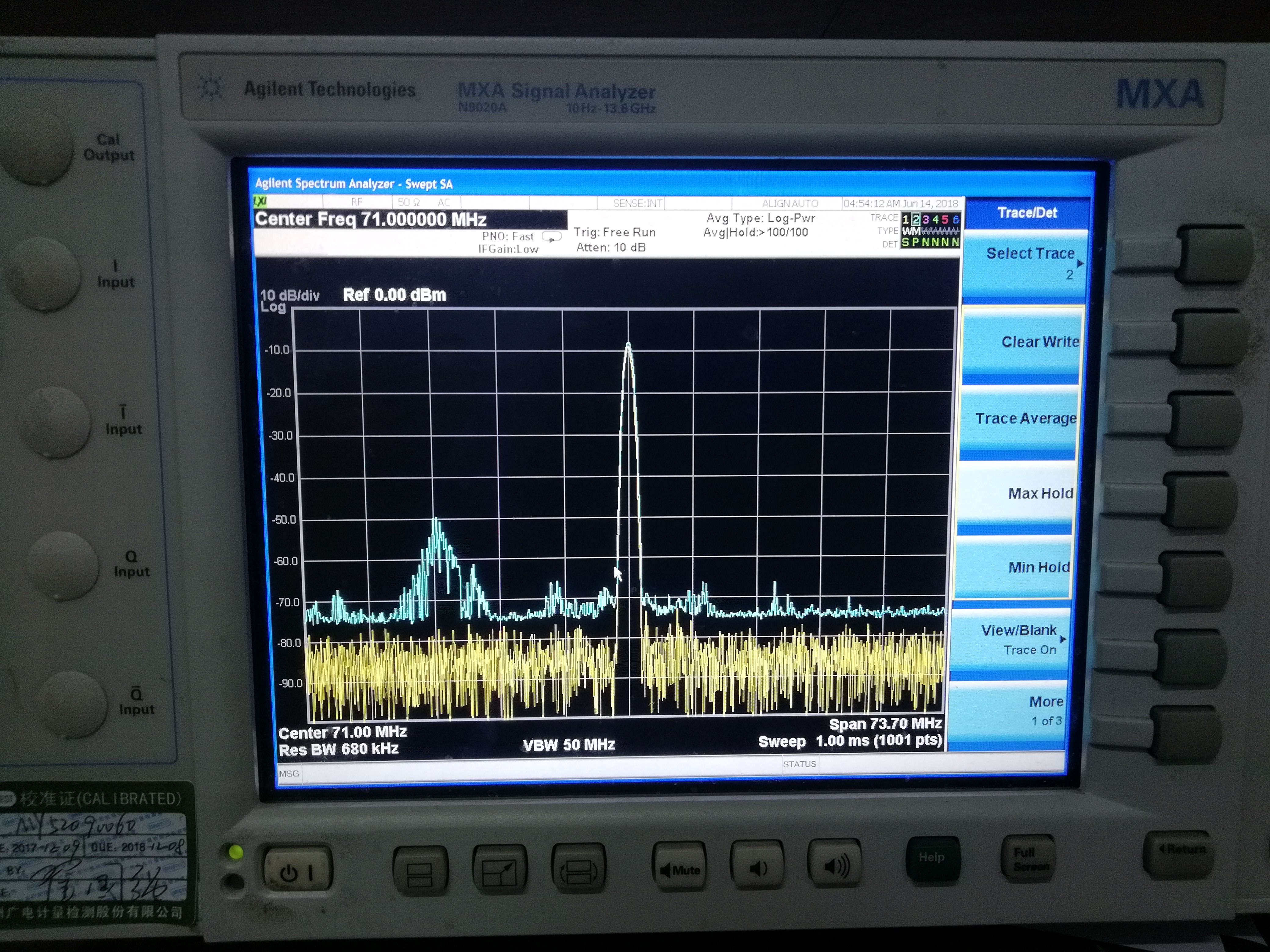
The current DTRU product uses DAC3482, with a failure rate of 12%, the IQ data from the FPGA side to DAC3482, the signal measured at the 3482 exit, and the presence of stray near the near end. As shown in the following figure.
In addition, the following experiments were done.
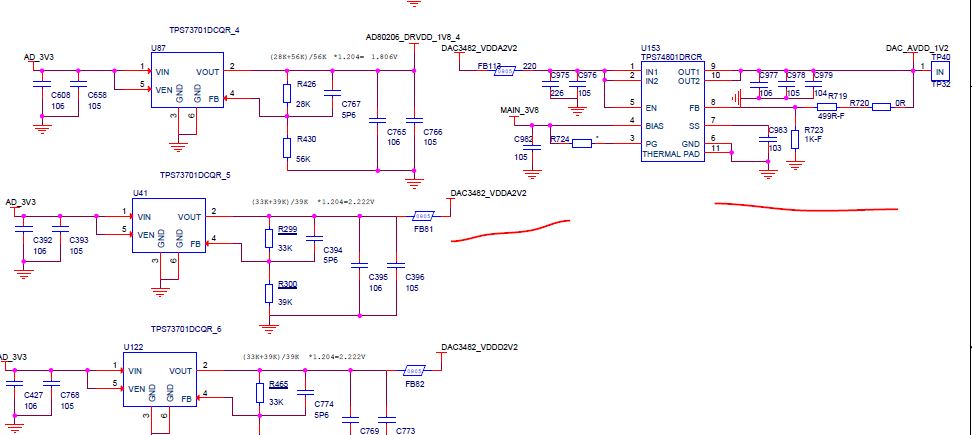
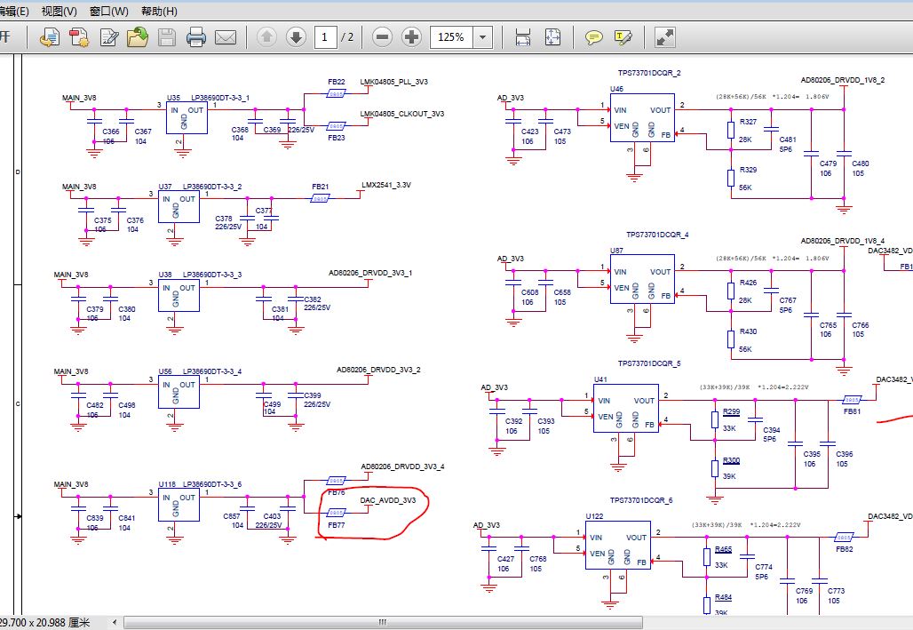
1, a good DTRU single board DAC3482_DIGVDD_1V2 is supplied to the DAC of the fault single board through the way of the external flight line, and the detection index of 10 fault single board is all OK, and no stray appears. After that, a good single board was used to supply the DAC of the fault veneer. A fault veneer was tested. It was found that there were still stray ends near the fault veneer.
2. After testing the DAC3482_DIGVDD_1V2 power chip (TPS74801) of a single board and a good single board, it is found that the good single board and the near end of the fault single board have been stray.
2) after adjusting the power chip, it is found that the good single board is still scattered at the near end.
3) pick up the new TPS74801 and paste it on the good veneer again, and find that the good veneer is still scattered near the end.
In addition, no matter how to adjust the FPGA terminal or the delay between the data and clock in the DAC3482 internal register terminal, it is impossible to eliminate the near end stray of the fault veneer.