This thread has been locked.

If you have a related question, please click the "Ask a related question" button in the top right corner. The newly created question will be automatically linked to this question.

ADS131A02: Initialization Issue

Part Number: ADS131A02

Original Question: https://e2e.ti.com/support/data_converters/precision_data_converters/f/73/t/653880

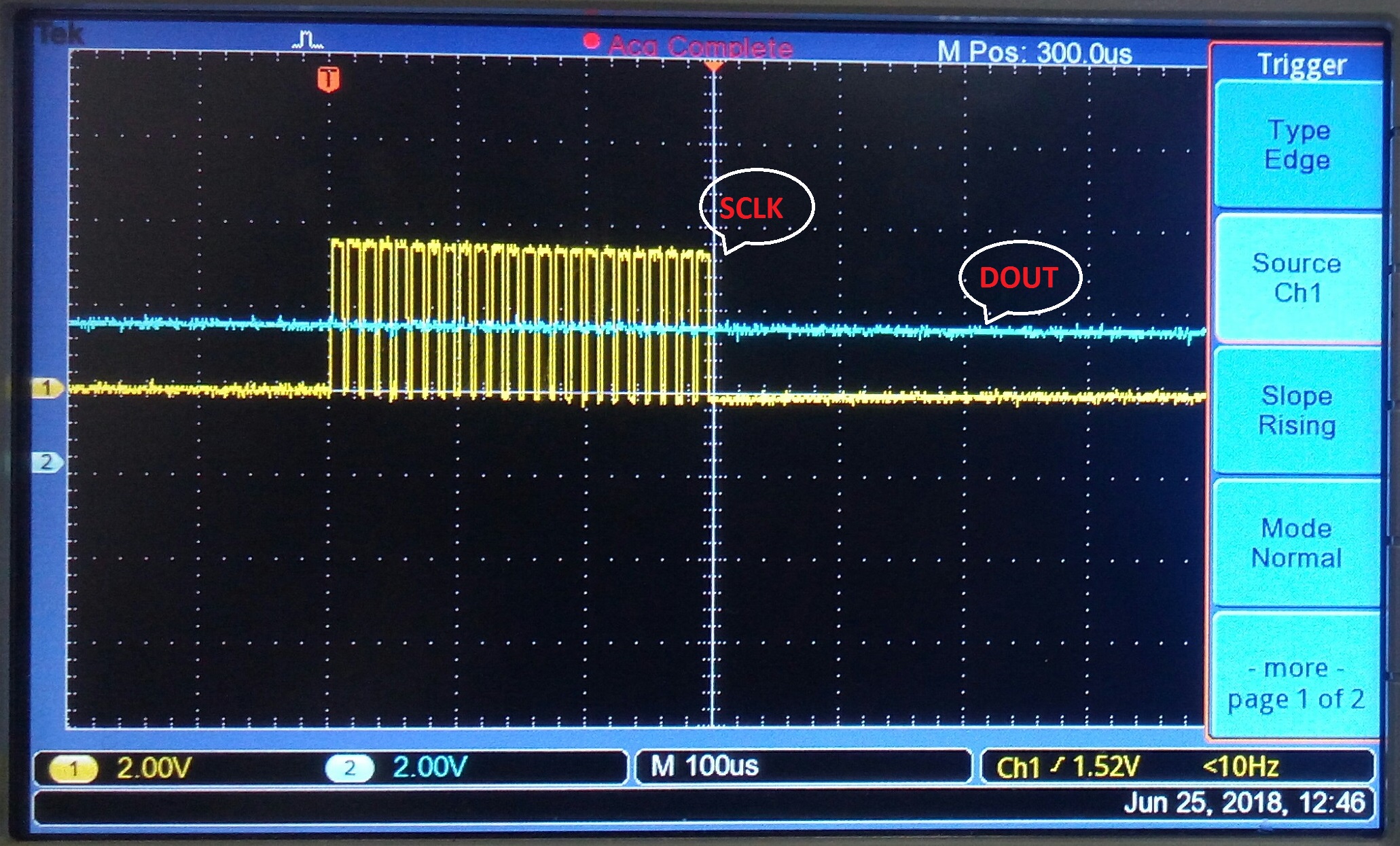
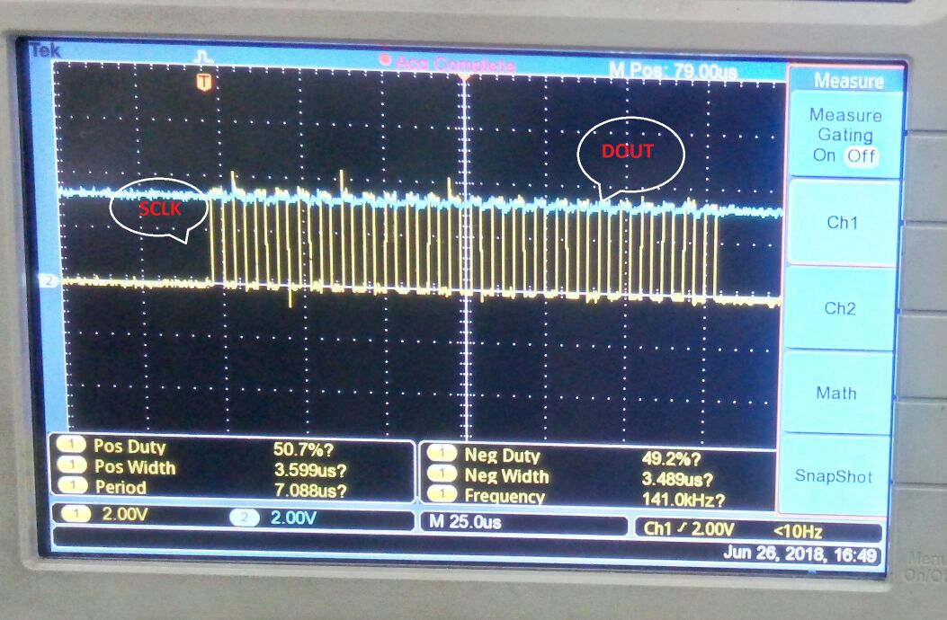
I am trying to initialize ADS131A02 as per the initialization process given in datasheet. First step mentioned in that is RESET. After sending RESET command (0x0011), ideally ADC should response a READY word (0xff02) but i am getting 0xffff(irrespective of data at DIN).

I am operating ADC in 24 bit mode & with 8Mhz external clock.

I am unable to recieve READY word.

Kindly help or share some sample code.

  • Hello Neha,

    Thank you for your post and welcome to our forum!

    Are you referring to Figure 106? During the initialization of the ADS131A02, the device cannot accept any commands until it is unlocked. "Reset" is mentioned in the fourth step to describe the status of the /RESET pin. This is meant to indicate that the /RESET pin should be high in order to initialize the device. You can use a pull-up resistor to connect /RESET to the digital supply so that it can ramp with the power supplies on your board. Can you check the /RESET pin after power-up and verify that it is high?

    The device should send the READY word automatically after the power supplies have ramped. You do not need to send any commands in order to see the READY word.

    *Edited 7/6/18: technically, the NULL command must be sent on DIN in order for the READY word to appear on DOUT*

    Best Regards,

  • Hello Ryan,

    Yes exactly, I am talking about figure 106. Currently RESET pin is pulled up to 3.3V(D) supply using a 10K resistor.

    Now according to you, I don't need to send any RESET command as ADC will automatically RESET when powered on. I just have to monitor READY word. 

    Am I getting right?

    Now I have checked the RESET pin on scope. Ideally it is low, as I powered on the device it goes high & then remains high.

  • Hi Neha,

    That is correct! The device automatically issues an internal power-on-reset (POR) as soon as the /RESET pin goes high and both power supplies have ramped.

    The next step is to wait for the READY command status response. Your start-up routine will need to repeatedly send the NULL command to the ADC until the READY word is received. Once you see the READY word, you can send the UNLOCK command. The response in the next frame will be 0655h to indicate the device is unlocked and ready to use.

    Best Regards,

  • Hi Ryan,

    I have tried the same way but failed to get READY response. DOUT pin is continuously high.

    Kindly check the attached files & inform me if m doing something wrong.

    #include �adc.h�
    
    void uiADC_WriteADCWord(uint32_t uiWordData)
    {
           uint8_t ucLoop=0;
    	defADC_ClrPinSCLK;
    	vDelay(2);
    	vSPI1_EnableSlave();
    	vDelay(2);
    	for(ucLoop=0;ucLoop<24;ucLoop++)
    	{
    		defADC_SetPinSCLK;
    		vDelay(2);
    		if((uiWordData & 0x800000) == 0x800000)
    		{
    			defADC_SetPinDIN;
    		}
    		else
    			defADC_ClrPinDIN;
    		vDelay(5);
    		defADC_ClrPinSCLK;
    		vDelay(2);
    		uiWordData = uiWordData << 1;	// Shift Left by 1 bit
    	}
    	vSPI1_DisableSlave();
    	vDelay(2);
    }
    
    uint32_t uiADC_ReadADCWord(void)
    {
    	uint8_t ucLoop=0;
    	uint16_t uiWordData=0;
    	defADC_ClrPinSCLK;
    	vDelay(2);
    	vSPI1_EnableSlave();
    	vDelay(2);
    	for(ucLoop=0;ucLoop<24;ucLoop++)
    	{
    		uiWordData = uiWordData<<1;
    		defADC_SetPinSCLK;
    		vDelay(2);
    		uiWordData = uiWordData | defADC_GetPinStatusDOUT;
    		vDelay(5);
    		defADC_ClrPinSCLK;
    		vDelay(2);
    	}
    	vSPI1_DisableSlave();
    	vDelay(2);
    	return uiWordData;
    }
    
    void vADC_Init(void)
    {
    	GPIO_InitTypeDef			GPIO_InitStructure;
    
    	RCC_APB2PeriphClockCmd(RCC_APB2Periph_GPIOA, ENABLE);
    	GPIO_InitStructure.GPIO_Pin 	= defADC_SCLKPin | defADC_DINPin | defADC_CSPin;
    	GPIO_InitStructure.GPIO_Speed 	= GPIO_Speed_50MHz;
    	GPIO_InitStructure.GPIO_Mode	= GPIO_Mode_Out_PP;
    	GPIO_Init(defADC_SPIPort, &GPIO_InitStructure);
    
    	GPIO_InitStructure.GPIO_Pin 	= defADC_DOUTPin;
    	GPIO_InitStructure.GPIO_Speed 	= GPIO_Speed_50MHz;
    	GPIO_InitStructure.GPIO_Mode 	= GPIO_Mode_IPU;
    	GPIO_Init(defADC_SPIPort, &GPIO_InitStructure);
    
    	GPIO_InitStructure.GPIO_Pin = defADC_CLKPin;
    	GPIO_InitStructure.GPIO_Speed = GPIO_Speed_50MHz;
    	GPIO_InitStructure.GPIO_Mode = GPIO_Mode_AF_PP;
    	GPIO_Init(defADC_SPIPort, &GPIO_InitStructure);
    
    	RCC_APB2PeriphClockCmd(RCC_APB2Periph_GPIOC, ENABLE);
    	GPIO_InitStructure.GPIO_Pin 	= defADC_DRDYPin | defADC_DONEPin;
    	GPIO_InitStructure.GPIO_Speed 	= GPIO_Speed_50MHz;
    	GPIO_InitStructure.GPIO_Mode 	= GPIO_Mode_IPU;
    	GPIO_Init(defADC_ControlPort, &GPIO_InitStructure);
    
    	GPIO_InitStructure.GPIO_Pin 	= defADC_RESETPin;
    	GPIO_InitStructure.GPIO_Speed 	= GPIO_Speed_50MHz;
    	GPIO_InitStructure.GPIO_Mode 	= GPIO_Mode_Out_PP;
    	GPIO_Init(defADC_ControlPort, &GPIO_InitStructure);
    
    	RCC_MCOConfig(RCC_MCO_HSI);     				//RCC_MCO_HSI
    	vSPI1_DisableSlave();
    	vDelay(5);
    	vSPI1_EnableSlave();
    }


    void vSPI1_EnableSlave(void)
    {
    	// Set slave CS pin low
    	defADC_SPIPort->BRR = defADC_CSPin;
    }
    void vSPI1_DisableSlave(void)
    {
    	// Set slave CS pin high
    	defADC_SPIPort->BSRR = defADC_CSPin;
    }
    
    #include "main.h"
    
    uint8_t   adc_flag=0;
    
    int main(void)
    {
    	uint32_t response=0;
    	SystemInit();                          		// To set mcu clock
    	vADC_Init();
    	systick_Init();
    	adc_flag = 1;
        	while(1)
        	{
        		if(adc_flag==1)
        		{
        			while(!(response == 0xff0200))
        			{
        				response = 0;
        				uiADC_WriteADCWord(0x000000);
        				response = uiADC_ReadADCWord();
        		}
        		uiADC_WriteADCWord(0x065500);
        		response = uiADC_ReadADCWord();
        		adc_flag = 0;
        	}
        }
    }


  • Hi Neha,

    Is it possible to capture two consecutive data frames with an oscilloscope? The first should show the NULL command being sent, and the second should show the ADC response. Please probe SCLK, DIN, DOUT.

    Also, how are M0 and M2 configured? If you have Hamming Code enabled, please try disabling it by tying M2 to ground.

    Best Regards,

  • Hello Ryan,

    M0 & M1 are grounded while M2 is connected with IOVdd pin (i.e. 3.3V Digital). I have sent NULL command (0x000000) at DIN & captured ADC response. I am still receiving 0xffffff at DOUT.

    Kindly check the scope traces & provide me a solution.

    Also check my hardware.

  • Hello Neha,

    Thanks for sharing the scope captures. I understand it may be difficult to capture consecutive frames together (i.e. UNLOCK command + NULL command to see the response). From what I can tell, 0x000000 is written to DIN and you see only 0xFFFFFF on DOUT. If this is consistent with what you see every frame, then there is certainly an issue.

    One thing that I just noticed is that your SCLK does not appear to have a 50/50 duty cycle. Can you verify the SCLK frequency and high/low times for me? They must agree with the Timing Requirements in Table 7.6:

    Best Regards,

  • Hello Ryan,
    I tried to get 50/50 duty cycle and I got these captures now.
    As you can see it's still responsing 0xFFFFFF.
    Kindly suggest something.
  • Hi Neha,

    Please confirm the M0, M1, and M2 settings again. I just realized that your schematic drawing does not match was you wrote in your earlier reply:

    neha yadav said:
    M0 & M1 are grounded while M2 is connected with IOVdd

    Best Regards,

  • Hello Ryan,

    I wrote wrong earlier. M0, M1 & M2 are as per schematic drawing.

    M0 is connected with IOVdd while M1 & M2 are grounded.

  • Hi Neha,

    Apologies that this is taking so long to find the issue. I'm still at a loss. I'm talking with my design team to see if we've possibly overlooked anything else.

    How many boards / ADS131A02 devices have you tried to communicate with?

    Best Regards,
  • Hello Ryan,

    If you have any sample code for this ADC, kindly provide me that.

    I have tried to communicate with 1 device.

  • Hi Neha,

    Please try one or two more devices if you can.

    May I contact you at the email address in your profile?

    Regards,

  • Hello Ryan,

    Yes I will try one more device tomorrow and will let you know the response.

    Yes you can contact me at ydv95neha@gmail.com .

  • Hello Ryan,

    I tried another device also. But I got same results.

    Kindly suggest something as it has already consumed a lot of time.

  • Hello Neha,

    I've reread our thread and one detail that I still haven't confirmed with you is whether or not you are toggling the /CS pin between frames. When I say to send UNLOCK "in the first frame" and look for "READY" in the next frame, the /CS pin must be taken high to end the first frame and return low to start the second frame. Otherwise, sending additional SCLKs without toggling /CS will look like one long frame to the part and you will not see the correct response. Please confirm that you are:

    1. Sending the correct number of bits per frame (i.e. [OP-CODE + CRC (if enabled) words] x 24 bits per word).
    2. Toggling /CS at the end of each frame.

    Although the channels are disabled by default upon power-up, you can probe the /DRDY pin to see if it is toggling, even before you send any commands. Can you check the /DRDY pin on the scope after power-up before you communicate with the device?

    Best Regards,