This thread has been locked.

If you have a related question, please click the "Ask a related question" button in the top right corner. The newly created question will be automatically linked to this question.

ADS114S08: System Monitor AVDD DVDD error

Part Number: ADS114S08
Other Parts Discussed in Thread: , ADS1220

Hi,

I would need advice on some behavior regarding system monitor readout during overvoltage on analog inputs.

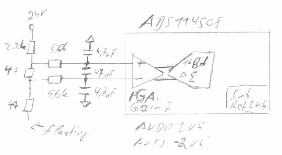
My setup is as follows:

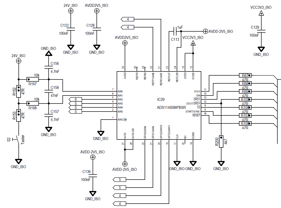
ADS114S08 with AVDD = +-2.5V, DVDD = 3,3V

RC low pass filter on all analog input pins with 10k Ohm resistor in series.

When 24V is applied on two analog inputs 3mA(total) input current is flowing.


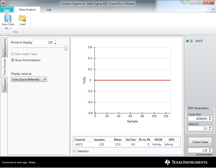
The device’s overall operation seems normal (inputs are at FSR), except the system monitor value for AVDD and DVDD indicates 0. The internal temperatur value is dropping(not 0).

I would not expect any change there. Can this be caused by an electrical problem?

I would appreciate any help, because after lots of software debugging I am running out of ideas.

Best regards

Daniel

  • Hi Daniel,

    Welcome to the E2E forum! It is not clear if the 24V input is a normal input voltage or if the system is such where 24V can be accidentally applied to the input.

    When 24V is applied to the input, you are exceeding or coming very close to the Absolute Maximum Ratings (section 7.1 on page 5 of the ADS114S08 datasheet.) See the accompanying note under the table in that section. You may not be over stressing the device, but you cannot assume the device will function normally. What you are doing is expecting the ESD structures (often considered as diodes) to protect the ADS114S08 by using the 10k resistor to limit current while using the ESD structure (that is meant for packaging and handling of the device) as a conduction path back to AVDD to lower the input voltage. In the case where 24V is applied, the input voltage at the pin is right at the AVDD +0.3V maximum. Current is back driving into the ADS114S08, and the internal current path within the device is unpredictable. This becomes an abnormal operating condition. The current limit prevents damage to the device, but the input voltage is still exceeding the Recommended Operating Conditions and operation may become unpredictable.

    I would not have expected that the System Monitor would act as you describe. However, without knowing the precise internal device current path it would be difficult to predict behavior, or if that behavior would act differently for different inputs or from device to device. In the end, I don't think you can rely on the functional operation of the ADS114S08 while in this condition.

    Best regards,
    Bob B
  • Hi Bob,

    thanks for your fast response. As far as I understand your answer we cannot expect the device to work properly as soon as current is flowing via the input protection circuitry of the device, which is at AVDD + 0.3V.

    We made a design according to 10.2 in the ADS114S08 datasheet. It could be worth mentioning there that the filter resistors only purpose is to protect the device from damage. And the function of the device may get unpredictable in this case.

    Best regards,

    Daniel

  • Hi Daniel,

    I'm not quite sure what your last post is trying to say.  The filter resistor has the primary purpose for filtering noise and to prevent aliasing.  In the application example in the ADS114S08 datasheet, the excitation source is the ADS114S08 and not from external sources.  In other words it cannot overdrive itself.  

    If there are large voltage spikes of noise from EMI, for example, then the diodes will help limit the effect to the IDACs and the filter resistors will have a secondary purpose of current limiting.

    Best regards,

    Bob B

  • Hi Bob,
    could you make a recommendation on how this problem could be solved.
    Best regards
    Daniel
  •  Hi Bob,

    I have made a little schematic of our application. In our error case we are doing a differential measurement over 47 Ohms. The input line is 24v over 2.2kOhm, 47Ohm, 47 Ohm floating GND (No GND connection). So the Input would see 24V if no current was drawn.

    The ADC inputs have a low pass filter with 10kOhms in series(5.6k in drawing is wrong). Internally the multiplexer connects the Input to the PGA with a gain setting of 2.

    In this case no internal measurement is correct. Some measurements are 0 some drop to lower value. In 10.2 in the datasheet is mentioned that the LP filter series resistor is also used to limit the current flowing into the device. Therefore we were expecting that the functionality of the rest of the channels would not be affected by the over voltage on one input.

    Can you make a suggestion on how to avoid this error?

    Best regards

    Daniel

  • Hi Daniel,

    With the 24V input, what is the input referring to (or what is it's 'ground' reference)? And how does this relate to the ADS114S08 AVDD/AVSS? To know the full affect of what is happening, I would need to know how the return current path for the 24V source as it flows through the ADS114S08. Is the 24V source connected to AGND? Also, why would the 47 ohm resistor be floating?

    Best regards,
    Bob B
  • Hi Bob,

    the GND reference for 24V, AVDD, AVSS, DVDD and IOVDD are the same. This GND is connected to AINCOM, DGND and CLK(for internal clock).

    The floating 47 Ohm covers one use case in which GND connection to this point is interrupted.

    Best regards

    Daniel

  • HI Bob,

    I made a better drawing. I hope this makes things a little clearer.

    Best regards

    Daniel

  • Hi Daniel,

    Sorry for the delayed response as USA had a national holiday yesterday. I think your new drawing is missing the 2.2k Ohm resistor to the 24V supply.

    I've got a question into our characterization team to see what testing may have been done similar to your application and reply again when I know more.

    I think the easiest thing would be to place S2 at the high-side. Another possible option would be to use a MOSFET switch in series with the input filters to open if a threshold greater than AVDD is seen.

    Best regards,
    Bob B
  • Hello Bob,

    in the meantime I was able to test the ADS114S08 on the TI EVM with Delta-Sigma ADC EvalutaTIon Software.

    Test setup is ADS114S08EVM with:

    • external Reference 2.5V
    • AVDD 3.3V
    • 10mA on (J9) Ain11
    • GND on ACOM (J9-3)
    • Differential input on Ain2 and Ain4 (J7)

    Findings are:

    • System monitor indicates wrong values on voltages above ca. AVDD+0,7V.
    • Current measurements are affected by overvoltage on some inputs (different from actual measurement input). If this happens, none of the measurements can be trusted.

    Pictrue shows (AVDD-AVSS)/4 with settigns shown above and 7V on (J7) Ain4 and GND on Ain2

    Picture showes 10mA current measurement on J9 Ain11 (1V is expected ) when 10V is applied to Ain4 and Ain2. . Approximately 2mA flows into each input.

    Our experience is based on ADS1220, which does not show this behavior regarding the system monitor. Does the ADS114S08 incorporate a totaly different technology? Is a hardware revision of the ADS114S08 scheduled?

    Best regards

    Daniel

  • Hi Daniel,

    I really don't know what more to tell you here.  You are exceeding the absolute maximum input voltage of the ADS114S08.  We don't expect the part to function correctly in this region.  Our validation does not check for correct operation outside of the normal operating region, so we don't know how the device will respond in this condition.  This could be an analog issue or a digital issue inside of the device.  Our validation does check for recovery and our testing shows that the ADS114S08 will recover when the device is returned to normal operating conditions.

    If you apply an over voltage condition to any input it will affect the others even though the MUX input for that channel is not selected due to internal devices and switches expecting to see voltages less than AVDD + 0.3V. 

    The ADS1220 and the ADS114S08 are totally different devices.  It is quite possible they behave differently.  There are no hardware changes planned for the ADS114S08.

    Best regards,

    Bob B

  • Hi Daniel,

    I just wanted to give you some more information regarding the differences in the ADS1220 and the ADS114S08 as it relates to monitoring the supplies. The monitor for the ADS1220 disables and bypasses the PGA whereas the ADS114S08 uses the PGA to make the measurement. Using the PGA allows for less current to be consumed in the resistor divider string used in the measurement.

    The ADS114S08 designer believes that the PGA is overloading when the input is driven overvoltage and that is why you are seeing a difference with this part versus the ADS1220 which is bypassing the PGA altogether in the measurement.

    As to the error shown on inputs not selected, the internal switches are not switches in the mechanical sense but rather MOSFET devices that can have leakage paths when voltages beyond the design are placed on the input(s). This leakage has unknown consequences, but due to the method and structures used can drive input common-modes outside of the PGA input range.

    Best regards,
    Bob B