This thread has been locked.

If you have a related question, please click the "Ask a related question" button in the top right corner. The newly created question will be automatically linked to this question.

DAC3482: The output of DAC3482 is lost after restarting it

Part Number: DAC3482
Other Parts Discussed in Thread: DAC3484, DAC38J84

Hi team,

My customer is using DAC3482 in a signal generator board. For some specific board, we found a strange phenomenon. At first, the DAC3482 works well. After it running for several minutes, we power down the board and power it up again, we found the DAC3482 output is lost. The input clk and FPGA input data are all existing. When we manually cool down the device and restart it, the DAC3482 output shows up again. This issue happend on 3 boards out of 10 boards.

The input clk is 500MHz. Interpolation=2. Data rate=500Msps. fdac=1GSPS 

We read out the reg values as below. The left column is read out when there's no output. The right column is read out when there is output.
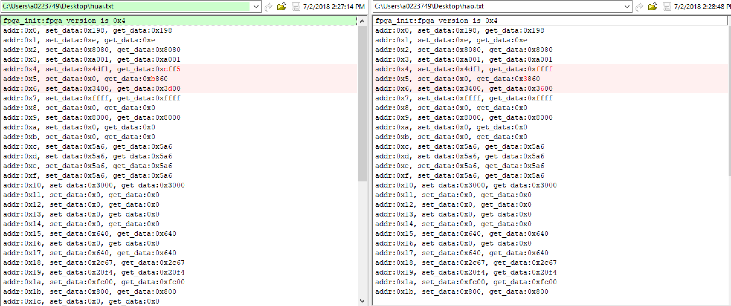
For reg 0x4, the value is different, but customer didn’t enable the “iotest_ena” in reg1. So why the value is different? Is this related to the output lost issue?

For reg 0x5, even in the right column(the DAC works well), the bit13-11 are all 1 which means “FIFO pointer collision alarm”. Do you think it is normal that this alarm happens when DAC3482 works well?

What’s more, in the left column, the bit 15 is 1 which is different from the right column. This means the alarm_from_zerochk. Do you think this is related to the output lost issue? If it is, how can we get rid of this alarm?

For reg 0x6, it means the temperature value read out. We read out the right column value after cooling the device down. So the value in right is smaller than left which is reansonable. But even when the output is lost, the tempertaure is not that high.

Hope you could help find out the root cause of the output lost issue. If you need more test results, please let me know. Thanks.

Best regards,

Wayne

  • Wayne,

    Usually when the registers are not reading back correctly or the FIFO collision alarm occurs, the power supply drop is the main cause. The power supply over the DC resistance drop, especially on DVDD rails, may need to be elevated to compensate for the IR drop.

    You may refer to the link below for guidance on using ATEST to check the internal nodes:

    For the register 0x04 of the IOTEST ena, I suspect this is due to the IR voltage drop causing the DAC to mis-behave, especially at hot temperature when the IR drop becomes more significant.

    For register 0x05, even for the DAC operating correctly, could they please make sure they clear all the alarms by writing zeros to the alarms registers before reading back the alarm. This will ensure the alarms reflect the latest operating status.

    For bit 15 with alarm from zero check, this means the FIFO input/output pointer is lost. There is no pointer in the FIFO, and this means fairly catastrophic event such as loss of power supply, which caused some flip-flops to have glitches. If some flip-flops inside the device has some glitches, then the FIFO pointers could be lost. Please double check the power supplies over temperature and over ATEST nodes.

    I see on-chip PLL is enabled, but the PLL loop filter voltage (LF_VOLT) is close to 7, which indicates close to unlocked. The pre-scaler is set to 4, which uses the 4GHz PLL range. This is on the higher end of the VCO range. I suggest the customer to try to set to 3GHz VCO with Pre-scaler = 3 to center the VCO range for flexibility. I also suggest the customer to review and double check the reference clock to the on-chip PLL is set correctly at all time to ensure good operation of the PLL.

    -Kang

  • Hi Kang,

    Thanks for your detailed explanation. I will ask customer to carefully check the power supply drop and feedback to you.

    But for your last point about the PLL setting. It seems that the output frequency of the VCO is designed to be the in the range from 3.3 GHz to 4.0 GHz. So it cannot be set to 3GHz. So could you please help recommond another proper setting of the PLL to stop it from unlocking? Thanks.

    Best regards,
    Wayne
  • Hi Wayne,

    You are correct. I got mixed up with other parts. The DAC3484 only support down to 3.3GHz, so 3GHz VCO is not possible.

    We will need to adjust the PLL_VCO(5:0) code perhaps from d59 to d64 within the range for each part and double check the loop filter voltage is optimal at room temp.
    For instance, we set to d60 and make sure the loop filter voltage read back is d4 (in the optimal range), and then set it for this part.
    other parts may have a different optimal setting
    This is the only way since we have to use the upper end of the VCO range. The upper/lower end of the VCO typically have higher variations. Unfortunately, we do not have screening program (like the newer DAC38j84) that offers exact code for the customer to use.

    -Kang