This thread has been locked.

If you have a related question, please click the "Ask a related question" button in the top right corner. The newly created question will be automatically linked to this question.

DAC8881: DAC does not output expected values

Part Number: DAC8881

For a project I'm working one I have to use two DAC's. I have chosen for the DAC8881 DAC.

No I encountered a problem that I do not quite understand why it happens, so I hope one of you can help me a step further.
(Let me note that I'm not a hardcore programmer)

The DAC8881 seems to me to be quite a simple DAC and so I didn't expect any problems. I know that the problem I have is something I do/did wrong but for some reason I can't figure out what it is.

The problem I have is this:
- When I send a value to the DAC it doesn't output what I expect it to do. The output doesn't seem to have any logical pattern.
The control seems to stop at 0x7FFF and does not follow a linear pattern from 0x0000 to 0x7FFF. 

Vref = 2.048V    (LM4132AMF-2.0)
AVDD = 3.3V
DVDD = 3.3V

Default hardware setting:

Default boot:
Vout = 0V (Register = 0000h) RSTSEL -> GND
PDN = GND -> device is never powered down
SDOSEL = IOVDD -> Device in standalone mode
GAIN = GND -> Gain = 1x
!LDAC = GND -> DAC value immediately updated
!RST = +3v3 -> Device never hardware reset, excl. power cycle
RSTSEL = GND -> sets the boot output voltage register to 0x0000 / 0V
USB/BTC = IOVDD -> Straight Binary Code output

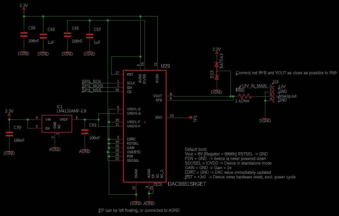
The circuit made is equivalent to: the Analog Output Closed-Loop Configuration shown in the datasheet on page 26. (on my board the RFB and Vout pins are connected at the point where the signal leaves the PCB)


Some Examples:  (Just for your information: the real output voltage measured with a Fluke 115)

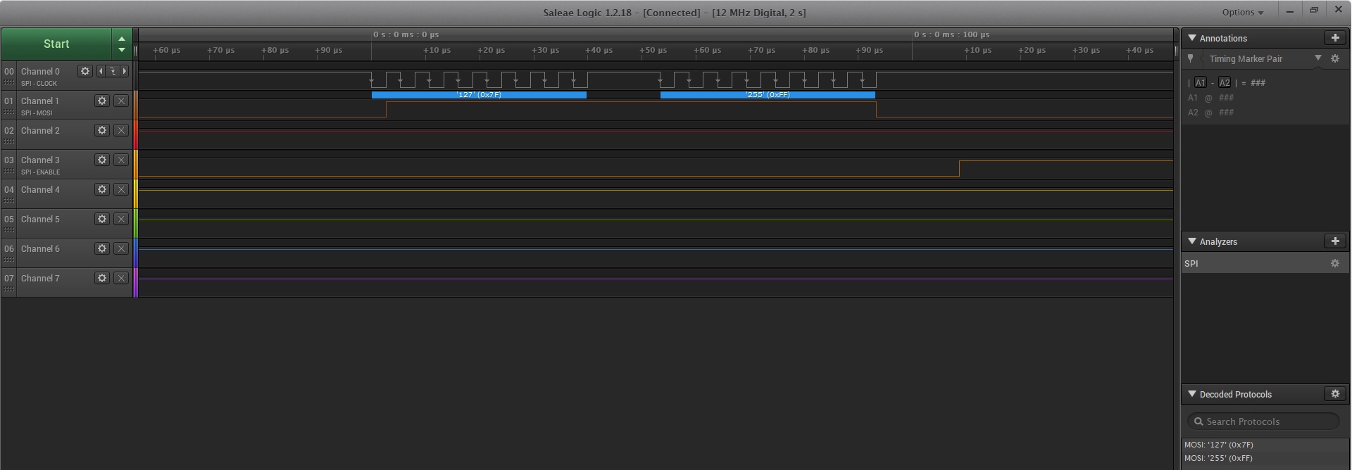
Send Code: (confirmed with Logic analyzer) 0x0C80 should be 0.1V at the output real output is: 0.064V
Send Code: (confirmed with Logic analyzer) 0x1900 should be 0.2V at the output real output is: 0.128V
Send Code: (confirmed with Logic analyzer) 0x2580 should be 0.3V at the output real output is: 0.008V
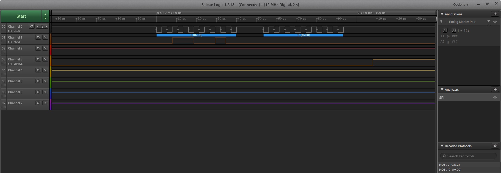
Send Code: (confirmed with Logic analyzer) 0x3200 should be 0.4V at the output real output is: 0.256V
Send Code: (confirmed with Logic analyzer) 0x3E80 should be 0.5V at the output real output is: 0.480V
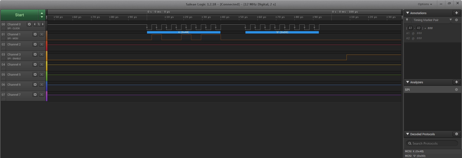
Send Code: (confirmed with Logic analyzer) 0x4B00 should be 0.6V at the output real output is: 0.016V
Send Code: (confirmed with Logic analyzer) 0x5780 should be 0.7V at the output real output is: 0.056V
Send Code: (confirmed with Logic analyzer) 0x6400 should be 0.8V at the output real output is: 0.512V
Send Code: (confirmed with Logic analyzer) 0x7080 should be 0.9V at the output real output is: 0.768V
Send Code: (confirmed with Logic analyzer) 0x7D00 should be 1.0V at the output real output is: 0.960V
Send Code: (confirmed with Logic analyzer) 0x7FFF should be 1.024V at the output real output is: 1.024V
Send Code: (confirmed with Logic analyzer) 0x8980 should be 1.1V at the output real output is: 0.008V
Send Code: (confirmed with Logic analyzer) 0x9600 should be 1.2V at the output real output is: 0.032V
Send Code: (confirmed with Logic analyzer) 0xA280 should be 1.3V at the output real output is: 0.004V
Send Code: (confirmed with Logic analyzer) 0xAF00 should be 1.4V at the output real output is: 0.112V
Send Code: (confirmed with Logic analyzer) 0xBB80 should be 1.5V at the output real output is: 0.408V
Send Code: (confirmed with Logic analyzer) 0xC800 should be 1.6V at the output real output is: 1.024V
Send Code: (confirmed with Logic analyzer) 0xD480 should be 1.7V at the output real output is: 1.024V
Send Code: (confirmed with Logic analyzer) 0xE100 should be 1.8V at the output real output is: 1.536V
Send Code: (confirmed with Logic analyzer) 0xED80 should be 1.9V at the output real output is: 1.608V
Send Code: (confirmed with Logic analyzer) 0xFA00 should be 2.0V at the output real output is: 1.919V
Send Code: (confirmed with Logic analyzer) 0xFFFF should be 2.048V at the output real output is: 2.047V

-----------------------------------------------------------------------------------------------------------------------------------------------
A Small snippet of the code:

void SendVoltageToDACValue(int setpoint, GPIO_TypeDef* GPIOx, uint16_t GPIO_Pin)
{

uint16_t DACValueToSend = 0;

DACValueToSend = setpoint;

SPI_DataToSend[0] = (uint8_t)((DACValueToSend & 0xFF00)>>8);
SPI_DataToSend[1] = (uint8_t)((DACValueToSend & 0x00FF));
digitalWrite(GPIOx, GPIO_Pin, LOW);

HAL_Delay(1);

HAL_SPI_Transmit(SPI_HANDLER, SPI_DataToSend, 2, SPI_TIMEOUT);

digitalWrite(GPIOx, GPIO_Pin, HIGH);

}

Do any of you have an Idea what the issue is here? I think it should be very simple but I just can't see it.


Thank you in advance for your time and effort 

  • JDW,

    I don't see the SPI configuration in your code snippet. Can you describe the clock phase and clock polarity settings you have configured the SPI bus with? Also the clock frequency? Even better would be to see oscilloscope captures of an SPI transaction on the bus (ideally just one frame so the resolution is sufficient to see details concerning the digital signals integrity).

    I know you have described the hardware in text, but most ideal would be to see a schematic since in the end this is most directly representative of the hardware. I think I'm less likely to miss a detail if reviewing the schematic directly. Being that the device seems mostly function I somewhat doubt this is a schematic issue.
  • Kevin,

    Thank you for your fast reply.

    Here is the data you asked for: (I don't have a oscilloscope capture available at the moment only a logic analyser capture, this because because our scope has some problems )

    ---------------------------------------------------------------  SPI configuration----------------------------------------------------------

    SPI_HandleTypeDef hspi1;
    
    /* SPI1 init function */
    void MX_SPI1_Init(void)
    {
    
      hspi1.Instance = SPI1;
      hspi1.Init.Mode = SPI_MODE_MASTER;
      hspi1.Init.Direction = SPI_DIRECTION_2LINES;
      hspi1.Init.DataSize = SPI_DATASIZE_8BIT;
      hspi1.Init.CLKPolarity = SPI_POLARITY_HIGH;
      hspi1.Init.CLKPhase = SPI_PHASE_1EDGE;
      hspi1.Init.NSS = SPI_NSS_SOFT;
      hspi1.Init.BaudRatePrescaler = SPI_BAUDRATEPRESCALER_256; // was 4
      hspi1.Init.FirstBit = SPI_FIRSTBIT_MSB;
      hspi1.Init.TIMode = SPI_TIMODE_DISABLE;
      hspi1.Init.CRCCalculation = SPI_CRCCALCULATION_DISABLE;
      hspi1.Init.CRCPolynomial = 7;
      hspi1.Init.CRCLength = SPI_CRC_LENGTH_DATASIZE;
      hspi1.Init.NSSPMode = SPI_NSS_PULSE_ENABLE;
      if (HAL_SPI_Init(&hspi1) != HAL_OK)
      {
        _Error_Handler(__FILE__, __LINE__);
      }
    
    }
    
    void HAL_SPI_MspInit(SPI_HandleTypeDef* spiHandle)
    {
    
      GPIO_InitTypeDef GPIO_InitStruct;
      if(spiHandle->Instance==SPI1)
      {
      /* USER CODE BEGIN SPI1_MspInit 0 */
    
      /* USER CODE END SPI1_MspInit 0 */
        /* SPI1 clock enable */
        __HAL_RCC_SPI1_CLK_ENABLE();
      
        /**SPI1 GPIO Configuration    
        PB3     ------> SPI1_SCK
        PB5     ------> SPI1_MOSI 
        */
        GPIO_InitStruct.Pin = GPIO_PIN_3|GPIO_PIN_5;
        GPIO_InitStruct.Mode = GPIO_MODE_AF_PP;
        GPIO_InitStruct.Pull = GPIO_NOPULL;
        GPIO_InitStruct.Speed = GPIO_SPEED_FREQ_HIGH;
        GPIO_InitStruct.Alternate = GPIO_AF0_SPI1;
        HAL_GPIO_Init(GPIOB, &GPIO_InitStruct);
    
        /* SPI1 interrupt Init */
        HAL_NVIC_SetPriority(SPI1_IRQn, 0, 0);
        HAL_NVIC_EnableIRQ(SPI1_IRQn);
      /* USER CODE BEGIN SPI1_MspInit 1 */
    
      /* USER CODE END SPI1_MspInit 1 */
      }
    }
    
    void HAL_SPI_MspDeInit(SPI_HandleTypeDef* spiHandle)
    {
    
      if(spiHandle->Instance==SPI1)
      {
      /* USER CODE BEGIN SPI1_MspDeInit 0 */
    
      /* USER CODE END SPI1_MspDeInit 0 */
        /* Peripheral clock disable */
        __HAL_RCC_SPI1_CLK_DISABLE();
      
        /**SPI1 GPIO Configuration    
        PB3     ------> SPI1_SCK
        PB5     ------> SPI1_MOSI 
        */
        HAL_GPIO_DeInit(GPIOB, GPIO_PIN_3|GPIO_PIN_5);
    
        /* SPI1 interrupt Deinit */
        HAL_NVIC_DisableIRQ(SPI1_IRQn);
      /* USER CODE BEGIN SPI1_MspDeInit 1 */
    
      /* USER CODE END SPI1_MspDeInit 1 */
      }
    } 

    ------------------------------------------------------------------------------------------------------------------------------------

    schematic:

    Logic analyser screen of command: 1.024V 0x7FFF

    Logic analyser screen of command: 0.6V 0x4B00 

    Logic analyser screen of command: 0.4V 0x3200

  • Goodday Kevin Duke,

    I already found the solution. One part of your reply made me test the clock polarity settings. I changed it from the (Default) HIGH to LOW and now the DAC works like a charm.
    I knew it would be something small and stupid causing the problem, your reply helped to point me in the right direction.

    Thank you, and have a nice day!
  • JDW,

    That is great news! Thank you for closing the loop and giving us the update on this thread.

    Please let us know if you need any assistance in the future on this project or the next.