Dear member of the support team,
I have been trying to get the following to work for quite a while now:
The ADS1118 shall operate to sense voltages of two Type-K-temperature sensors, connected to the differential inputs of the ADC.
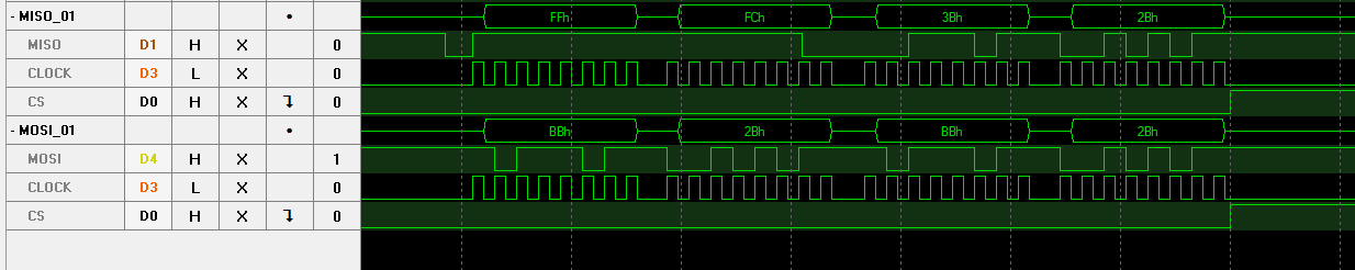
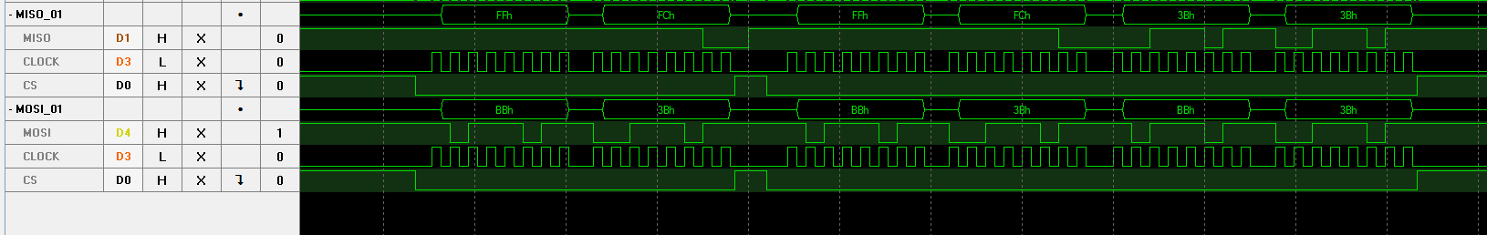
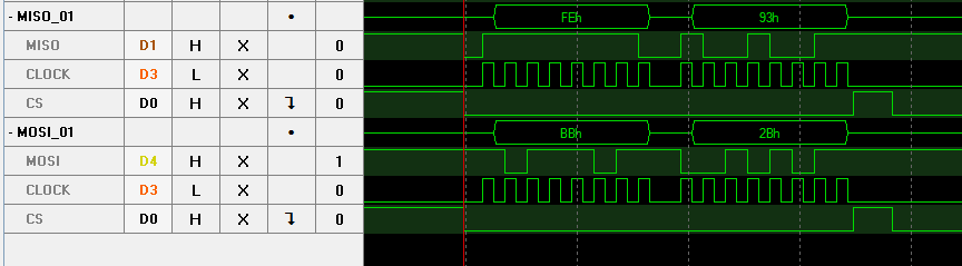
The communication via SPI seems not to work properly. As can be seen in the CommFailX.png files, the logic analyser indicates the correct command being sent by the µC. The ADS1118 does not repeat the correct Configuration Bytes as can be seen in the Logic Analyser’s scope within the 32Bit communication cycle. Another thing that is confusing is that the first failure reveals a waiting time of about 60ms for the conversion to take place, because of which I needed to split the scope, otherwise the display wouldn’t have granted a reasonable overview. I guess there is some other thing that is strange here since this is way more than the 20µs you proposed in one of your forum answers.
Find the minimal work example I used attached. The code runs on a ATMEGA8A, CPU clock is crystal-stabilised at 8MHz. Find the schematic attached as well.
Thanks a lot for your attention. I hope you can help me concerning this issue.
Kind regards,
Daniel Philipps
ADS1118Conn.schADS1118Conn.brd
/**from main.c:**/

#define F_CPU 8000000UL
#define TRUE 1
#define FALSE 0


#inlcude “SPIinit.h”
#include “tempADS1118.h“
#include <stdint.h>
#include <util/delay.h>
#include <avr/io.h>
#include <avr/interrupt.h>
#include <stdlib.h>
//(...)
void initialise(){
  spiInit(SPI_MODE_1, SPI_MSB, SPI_NO_INTERRUPT,  SPI_MSTR_CLK32);
  _delay_ms(500);
}
//(...)
int main(void)
{
  initialise();
  float temp1, temp2, temp3, temp4
  while (1) {
    _delay_ms(500);
    temp1 = perform16BitMeasurement(ADS_DEFAULT_CONFIG_LINKS);
    _delay_us(100);
    temp2 = perform16BitMeasurement(ADS_DEFAULT_CONFIG_LINKS_INT);
    _delay_us(100);
    temp3 = perform16BitMeasurement(ADS_DEFAULT_CONFIG_RECHTS);
    _delay_us(100);
    temp4 = perform16BitMeasurement(ADS_DEFAULT_CONFIG_RECHTS_INT);
    _delay_ms(500);
  }
}


/**From SPIinit.h:**/


#ifndef TRUE
#define TRUE 1
#endif

#ifndef FALSE
#define FALSE 0
#endif


#include <avr/io.h>
#include <avr/interrupt.h>
#include <stdint.h>
#include <util/delay.h>
#include <stdlib.h>

#ifndef SPIINIT_H_
#define SPIINIT_H_

//PinDef
#define SPI_SS_STAT_REG PINB
#define SPI_SS_PORT PORTB
#define SPI_SS_PIN PORTB2
#define SPI_SCK_PIN PORTB5
#define SPI_MOSI_PIN PORTB3
#define SPI_MISO_PIN PORTB4

//SPI clock modes
#define SPI_MODE_0 0x00 /* Sample (Rising) Setup (Falling) CPOL=0, CPHA=0 */
#define SPI_MODE_1 0x01 /* Setup (Rising) Sample (Falling) CPOL=0, CPHA=1 */
#define SPI_MODE_2 0x02 /* Sample (Falling) Setup (Rising) CPOL=1, CPHA=0 */
#define SPI_MODE_3 0x03 /* Setup (Falling) Sample (Rising) CPOL=1, CPHA=1 */

// data direction
#define SPI_LSB 1 /* LSB first */
#define SPI_MSB 0 /* MSB first */

// Interrupt when data received (SPIF bit received)
#define SPI_NO_INTERRUPT 0
#define SPI_INTERRUPT 1

// slave or master with clock div
#define SPI_SLAVE 0xF0
#define SPI_MSTR_CLK2 0x04 /* chip clock/2 */
#define SPI_MSTR_CLK4 0x00 /* chip clock/4 */
#define SPI_MSTR_CLK16 0x01 /* chip clock/16 */
#define SPI_MSTR_CLK64 0x02 /* chip clock/64 */
#define SPI_MSTR_CLK128 0x03 /* chip clock/128 */
#define SPI_MSTR_CLK2 0x04 /* chip clock/2 */
#define SPI_MSTR_CLK8 0x05 /* chip clock/8 */
#define SPI_MSTR_CLK32 0x06 /* chip clock/32 */

void spiInit(  uint8_t mode,      // timing mode SPI_MODE[0-4]
        uint8_t dord,             // data direction SPI_LSB|SPI_MSB
        uint8_t interruptEnable, // whether to raise interrupt on recieve
        uint8_t msClock); // clock diviser

uint8_t spiTransceiveByte(uint8_t data, uint8_t eot);

#endif


/**From SPIinit.c:**/


#include "SPIinit.h"

//initialise the SPI Bus
void spiInit(uint8_t mode, uint8_t dord, uint8_t interruptEnable, uint8_t msClock)
{
  // specify pin directions for SPI pins on port B
  if (msClock == SPI_SLAVE) {            // if slave SS and SCK is input
    DDRB &= ~(1<<SPI_MOSI_PIN);          // input
    DDRB |= (1<<SPI_MISO_PIN);          // output
    DDRB &= ~(1<<SPI_SS_PIN);          // input
    DDRB &= ~(1<<SPI_SCK_PIN);          // input
    } else {
    DDRB |= (1<<SPI_MOSI_PIN);          // output
    DDRB &= ~(1<<SPI_MISO_PIN);          // input
    DDRB |= (1<<SPI_SCK_PIN);          // output
    DDRB |= (1<<SPI_SS_PIN);          // output
  }
  SPCR = ((interruptEnable ? 1 : 0)<<SPIE)    // interrupt enabled
  | (dord<<DORD)                  // LSB or MSB
  | (((msClock != SPI_SLAVE) ? 1 : 0) <<MSTR)    // Slave or Master
  | (((mode & 0x02) == 2) << CPOL)        // clock timing mode CPOL
  | (((mode & 0x01)) << CPHA)            // clock timing mode CPHA
  | (((msClock & 0x02) == 2) << SPR1)        // cpu clock divisor SPR1
  | ((msClock & 0x01) << SPR0);          // cpu clock divisor SPR0


  SPSR = (((msClock & 0x04) == 4) << SPI2X);    // clock divisor SPI2X

  SPCR |= (1<<SPE); //enable SPI
}

uint8_t spiTransceiveByte(uint8_t data, uint8_t eot){
  //pull down the slave select pin
  SPI_SS_PORT &= ~(1<<SPI_SS_PIN);
  _delay_us(10);

  // Load data into the buffer
  SPDR = data;

  //Wait until transmission complete
  while(!(SPSR & (1<<SPIF)));

  //if end of transmission is reached, pull up the ssPin
  if(eot)  SPI_SS_PORT |= (1<<SPI_SS_PIN);

  // Return received data
  return SPDR;
}


/**From  tempADS1118.h:**/


#include "SPIinit.h"
#include <stdlib.h>
#include <util/delay.h>
#include <stdint.h>

#ifndef TRUE
#define TRUE 1
#endif

#ifndef FALSE
#define FALSE 0
#endif


#ifndef TEMPADS1118_H_
#define TEMPADS1118_H_


/* left ext sense
 * SingleShot (SS)
 * default MUX to left (MUX = 000; default)
 * lowest amplification (e.g. PGA = 101)
 * SingleShot + PowerDown (MODE = 1)
 * 16SPS DataRate (DR = 001)
 * ADC mode (TS_MODE = 0; default)
 * internal pullup resistor (PULL_UP_EN = 1)
 * no operation (NOP = 01) otherwise failure
 * Reserved always 1 (R=1)
 */

#define ADS_DEFAULT_CONFIG_LINKS 0b1000101100101011//1 000 101 1 001 0 1 01 1


/* right ext sense
 * SingleShot (SS)
 * MUX to right (MUX = 011)
 * lowest amplification (e.g. PGA = 101)
 * SingleShot + PowerDown (MODE = 1)
 * 16SPS DataRate (DR = 001)
 * internal pullup resistor (PULL_UP_EN = 1)
 * no operation (NOP = 01) otherwise failure
 * Reserved always 1 (R=1)
 * ADC mode (TS_MODE = 0; default)
 */

#define ADS_DEFAULT_CONFIG_RECHTS 0b1011101100101011//1 011 101 1 001 0 1 01 1


/* left int sense
 * SingleShot (SS)
 * MUX to left (MUX = 000; default)
 * lowest amplification (e.g. PGA = 101)
 * SingleShot + PowerDown (MODE = 1)
 * 16SPS DataRate (DR = 001)
 * internal pullup resistor (PULL_UP_EN = 1)
 * no operation (NOP = 01) otherwise failure
 * Reserved always 1 (R=1)
 * Tsense mode (TS_MODE = 0)
 */

#define ADS_DEFAULT_CONFIG_LINKS_INT 0b1000101100111011 //1 000 101 1 001 1 1 01 1


/* right int sense
 * SingleShot (SS)
 * MUX to right (MUX = 011)
 * lowest amplification (e.g. PGA = 101)
 * SingleShot + PowerDown (MODE = 1)
 * 16SPS DataRate (DR = 001)
 * Tsense mode (TS_MODE = 1)
 * internal pullup resistor (PULL_UP_EN = 1)
 * no operation (NOP = 01) otherwise failure
 * Reserved always 1 (R=1)
 */

#define ADS_DEFAULT_CONFIG_RECHTS_INT 0b1011101100111011 //1 011 101 1 001 1 1 01 1


#define ADS_DEFAULT_CONFIG_T0    ADS_DEFAULT_CONFIG_LINKS
#define ADS_DEFAULT_CONFIG_T0_INT  ADS_DEFAULT_CONFIG_LINKS_INT
#define ADS_DEFAULT_CONFIG_T1    ADS_DEFAULT_CONFIG_RECHTS
#define ADS_DEFAULT_CONFIG_T1_INT  ADS_DEFAULT_CONFIG_RECHTS_INT


//perform one 16Bit Measurement (which is the measurement size of our ADC)
uint16_t perform16BitMeasurement(uint16_t valueMsg);

#endif /* TEMPADS1118_H_ */


/**From tempADS1118.c:**/

#include "tempADS1118.h"

//perform one 16Bit Measurement (which is the measurement size of the ADC)
uint16_t perform16BitMeasurement(uint16_t valueMsg){
	//request measurement
	uint8_t msgP1 = (uint8_t) (valueMsg >> 8); //MSB
	uint8_t msgP2 = valueMsg % 256 ; //LSB


	spiTransceiveByte(msgP1, FALSE);
	spiTransceiveByte(msgP2, TRUE);

	_delay_us(50);

	SPI_SS_PORT &= ~(1<<SPI_SS_PIN);
	//wait for conversion to be complete => MISO is pulled down
	while(PINB & (1<<PINB4));

	//receive value (16bit = 2Byte); MSB first - shift - LSB
	uint8_t valP1 = 0;
	uint8_t valP2 = 0;
uint16_t value = 0;
	valP1 = (uint16_t)spiTransceiveByte(msgP1, FALSE);
	valP2 = (uint16_t)spiTransceiveByte(msgP2, FALSE);
	spiTransceiveByte(msgP1, FALSE);
	spiTransceiveByte(msgP2, TRUE);


	value = valP1 << 8 + valP2;

	return value;
}