This thread has been locked.

If you have a related question, please click the "Ask a related question" button in the top right corner. The newly created question will be automatically linked to this question.

ADS1262: ADS1262 : Noise Issue

Part Number: ADS1262

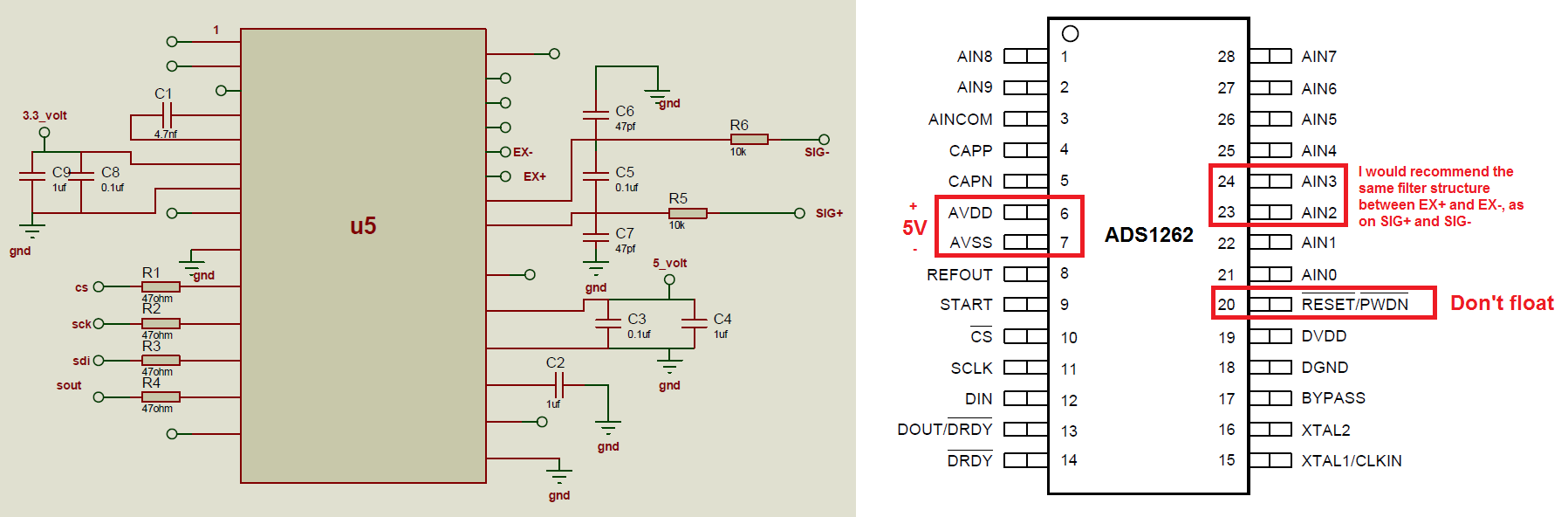
we are evaluating ADS1262 for accurate weighing measurement, we are getting accurate result but last 2 or 3 digits fluctuating  after 300,000 counts and taking time to get it stable so it seems like we are facing some noise issue, can you please recommend us a proper schematic or any change required in PCB layout? we are referring TICD188 for this. 

I have attached Schematic, Gerber, ADC Code and  have also attached small Demo video, which will help you to understand the issue. 
ads1262_data.rar
  • Hi Arpit,

    Welcome to the TI E2E Forums!

    When the data is settled, the noise performance looks pretty good, 1-2 count flicker as you mentioned. It's hard to say if that performance can be improved by much.

    However, what is more concerning are the temporary spikes in the data, where the display appears to be unsettled. That could be caused by a few different things:

    1. Any vibrations in the room or on the table, might couple into the load cell and cause results to be temporarily unsettled.
    2. EMI signals coupling into your system could also temporarily disturb the conversion result. Shielding your cables and PCB, or filtering out EMI signals might help.
    3. From the schematic, I see that the nRESET/nPWDN pin is floating. If any disturbances (EMI/capacitive coupling/leakage) cause that pin to toggle, it will certainly disturb the result.

    I reviewed your schematic and layout and have a few comments:

    • AVDD/AVSS should be a 5V supply, not 3.3V...Am I interpreting the schematic correctly? I'm assuming pins are shown in sequence, since only pin 1 was labelled.
    • Don't float nRESET/nPWDN as this need to be fixed HIGH for the device to operate.
    • Filtering the reference voltage might help to improve noise. I generally recommend using the exact same filters on the inputs and reference to allow for the best ratiometric noise cancellation.


    • The green layer appears to be the ground plane that is below the ADS1262. I see that there are traces routed on the ground plane layer which form ground plane cutouts. These cutoffs may restrict the flow of return currents on the ground plane. Also if any traces on the top layer are routed over these cutouts, they will tend to be much more inductive in behavior. I would recommend to avoid routing traces on the ground plane layer, if possible. If you only have two PCB layers to work with, then you have to be especially careful of where these traces are placed to ensure they don't disturb the natural return current flow below traces on the opposite layer.

    Other that those suggestions, reducing the data rate would be the other thing you could try to see if it helps to remove the display flicker and improve the noise performance.

    Best regards,
    Chris

    • Hi Chris,

      Thanks for providing your valuable input, our team is already working on the changes you suggested..

      We will conform you soon updated results..