This thread has been locked.

If you have a related question, please click the "Ask a related question" button in the top right corner. The newly created question will be automatically linked to this question.

ADS1256: Parallel ADCs

Part Number: ADS1256
Other Parts Discussed in Thread: LM1085

Hello,

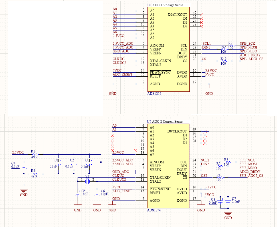
I am currently working on a design that uses two parallel ADS1256 chips to measure signals simultaneously.

The process of two ADCs simultaneously reading is listed below:

1. WREG channel to Mux Reg of both ADCs

2. Send SYNC commands to both ADCs

3. Send WAKEUP commands to both ADCs

4. Wait for DRDY of ADC1 to be low, then send RDATA command to ADC1

5. Wait for DRDY of ADC2 to be low, then send RDATA command to ADC2

Between each process of reading the same channel, there can be 0.2mV reading spike.

As far as the circuit setup goes the ADCs share the same crystal (7.68MHz). The

SPI Bus is shared between the two (chip select and data ready are separated). AIN COM and VREFP are tied to 2.5V and this is also shared between the two ADCs.

sampling rate: 60SPS

Input buffer: Off

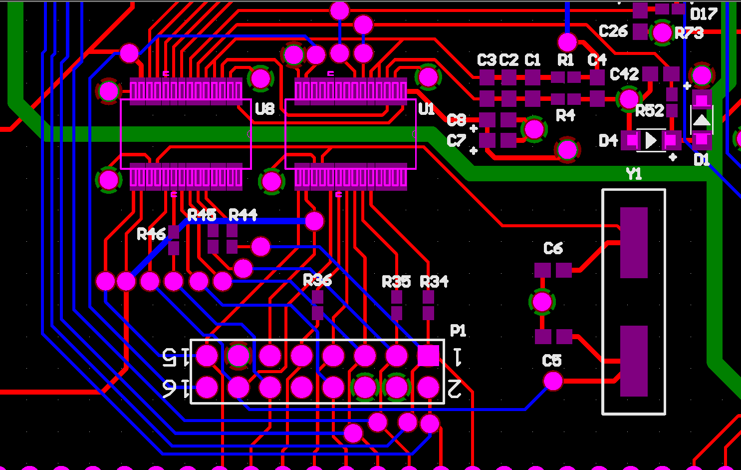
I do have a ground plane split underneath of the two ADCs separating the digital side and the analog side but they tie back together at another section of the PCB. I was wondering if you could provide some advice for minimizing noise while operating two parallel ADCs or specific device considerations that I might have missed?

Thanks for your time,

Mike

  • Hi Mike,

    I have several layout suggestions that I would like to mention, but I would also like to understand the conditions you used to measure the ADC's noise performance...

    • Was the noise test performed with an external DC signal, or with the ADC inputs shorted?
    • What are you using to generate the 2.5V reference voltage?
    • Also, which gain setting were you using?

    ...I ask in order to better compare your results to the datasheet's noise specifications, which assume that the inputs are shorted. If you were to measure the noise of the external DC signal, then we'd also need to know the amount of noise present in the signal source and reference voltage to know whether the noise was coming from the ADC or not.


    After reviewing your layout, I believe you will have higher than expected noise, even with the ADC inputs shorted. There are several things you can do to improve the noise performance in your system:

    Regarding the split ground plane...
    We generally discourage splitting the ground plane at all if it can be avoided. Split grounds plane can be used, but there are some additional rules that need to be followed, such as making sure to connect the analog and digital ground regions under the ADCs and never routing traces over the ground plane cutouts, as this makes traces highly inductive and more susceptible to voltage spikes. Using a single ground plane makes it easier to follow these rules and also avoids forming the ground plane into the same shape as a dipole antenna.

    Supply decoupling
    U1 has an AVDD supply decoupling capacitor near the IC, but U8's AVDD supply decoupling is far away. Try to move C7 or C8 closer to U8. Also U1 and U8 are both missing supply decoupling capacitors on DVDD. If no room can be made on the top layer, then add these decoupling caps on the bottom layer near the DVDD and DGND pins.

    Clocking and clock trace routing
    I would not recommend sharing a single crystal between ADCs. Likely this configuration will work okay once the crystal is oscillating; however, I would be concerned that a crystal connected to two crystal drivers might encounter issues during start-up where the crystal fails to oscillate. In this situation, I would recommend replacing the crystal with a crystal oscillator (an IC that combines the crystal and crystal driver circuitry and outputs a clock signal directly). A crystal oscillator will be much more likely to start-up correctly and will only require one clock trace to be routed to each ADC. In the current layout, the crystal traces form a large loop which may be susceptible to noise pick-up (especially since one of the traces is routed below other digital signals) and this loop may also radiate EMI noise.

    Input and reference filtering
    As much as possible, try to place the differential filtering capacitors between input and reference pins close to the ADC. This maximizes the effectiveness of filtering capacitors.

    Clock trace routing
    Try to avoid routing clock traces above or below other traces, and avoid using vias on clock traces since they add additional trace inductance. Clock traces typically have very fast edges and these signals can capacitively couple into nearby traces or result in voltage spikes when flowing through inductive traces. I often recommend that clock traces be routed first, so as to keep them short and routed on the same layer, and then other digital traces routed around the clock traces.

    I hope that feedback helps!

    Best regards,
    Chris

  • Hello Chris,

    Thank you for your detailed reply it is greatly appreciated. To answer your questions

    Q) Was the noise test performed with an external DC signal, or with the ADC inputs shorted?

    A: The noise test was performed with a 2.5Volt signal from a low dropout regulator (LM1085) on the PCB into Channel 7of the ADC. I also swapped out this    regulator network and used a MAX6325 voltage reference but it did not seem to have any affect positive or negative on the performance.

    Q) What are you using to generate the 2.5V reference voltage?

    A:  LM1085 voltage regulator (only tantalum capacitors used on output and input).

    Q) Also, which gain setting were you using?

    A:  PGA 2

    After reviewing your advice I decided that the best option is to re-organize the ADC connections and layout according to your recommendations to see if the performance of the ADC can be improved.

    Thank you very much for your help!

    Michael

  • Hi Micheal,

    Glad to help! Here are a couple more suggestions...


    Michael Buck said:
    A: The noise test was performed with a 2.5Volt signal from a low dropout regulator (LM1085) on the PCB into Channel 7of the ADC. I also swapped out this    regulator network and used a MAX6325 voltage reference but it did not seem to have any affect positive or negative on the performance.

    Have you tried shorting the differential inputs to to this 2.5V source and measuring the noise?

    I'd recommend measuring the noise with the inputs shorted (as close to 0V input as you can get) so as mimic the same test conditions that were used when the device noise was measured for the datasheet. Under this condition you'll be able to see the noise of the ADC without the effects of the input signal noise. It was also give you an idea of how much improvement in noise performance you stand to gain from trying to optimize the layout.


    Michael Buck said:
    A:  LM1085 voltage regulator (only tantalum capacitors used on output and input).

    Consider using a low-noise reference source, such as the REF5025...

    The ADC compares the input signal to the reference voltage, and provides an output code that is proportional to this ratio. In order to achieve  high-resolution, it is important to keep both of these signals as free from noise as possible. Note that the ratio (VIN + VIN_NOISE) / ( 2*VREF + VREF_NOISE) will be more sensitive to reference noise as VIN approaches VREF.

    Ignoring the ADC noise and only considering the effects of the reference source noise when VIN = 2*VREF, here is a simplified comparison of what you might expect for resolution using the LM1085 vs the REF5025:

    LM1085: 10 - 10,000 Hz noise is 0.003% * 2.5Vout = 75 uVrms, which means the ADC's effective resolution cannot exceed log2( 5 / 75 uVrms ) = 16 bits

    REF5025: 10 - 10,000 Hz noise (estimated) is about 7.6 uVrms, which means the ADC's effective resolution cannot exceed log2( 5 / 7.6 uVrms ) = 19.3 bits

    In practice you'll have other sources of noise and the digital filter will also help to reduce the noise bandwidth and overall noise; however, as a point of reference you can see that the resolution might be as much as 10x times better using the REF5025.

    Best regards,
    Chris