Other Parts Discussed in Thread: ADS114S08, ADS114S08B, ADS124S08
Tool/software: Code Composer Studio
I use J3 on board to be able communicate with ADS114S08 through SPI. The external processor that I use is TIVA TM4C129NCPD. I use the RTD (3-WIRE one ) channel of the board and connected a resistor between AN1-AN2.
First, I initialized the SSI0 module executing InitSSI function as,
void InitSSI(void)
{
uint32_t extra;
SysCtlClockFreqSet((SYSCTL_XTAL_25MHZ | SYSCTL_OSC_MAIN | SYSCTL_USE_PLL | SYSCTL_CFG_VCO_480), SYS_CLK_FREQ);
SysCtlPeripheralEnable(SYSCTL_PERIPH_SSI0);
SysCtlPeripheralEnable(SYSCTL_PERIPH_GPIOA);
GPIOPinConfigure(GPIO_PA2_SSI0CLK); // SSI module 0 clock
GPIOPinConfigure(GPIO_PA3_SSI0FSS); // SSI module 0 frame signal
GPIOPinConfigure(GPIO_PA4_SSI0XDAT0); // SSI Module 0 Bi-directional Data Pin 0 (SSI0TX in Legacy SSI Mode).
GPIOPinConfigure(GPIO_PA5_SSI0XDAT1); // SSI Module 0 Bi-directional Data Pin 1 (SSI0RX in Legacy SSI Mode).
GPIOPinTypeSSI(GPIO_PORTA_BASE, GPIO_PIN_5 | GPIO_PIN_4 | GPIO_PIN_3 | GPIO_PIN_2);
SSIConfigSetExpClk(SSI0_BASE, SYS_CLK_FREQ, SSI_FRF_MOTO_MODE_1, SSI_MODE_MASTER, 10000000, 8);
SSIEnable(SSI0_BASE);
while(SSIDataGetNonBlocking(SSI0_BASE, &extra)){ }
}
With settings above I was able to send data to the ADS114S08 succesfully. To initialize the ADS114S08 I executed Init_ADS114S08_RTD function as,
//*******************************************************
// ADS114S08B Definitions
//*******************************************************
#define RTD_START_COMMAND 0x08 // SPI data to start new conversion in ADS114S08
#define RTD_CH1_INPUTMUX 0x12 // SPI data to set AIN1 and AIN2 as positive and negative input selections, respectively.
#define RTD_CH1_IDACMUX 0x35 // SPI data to set AIN5 and AIN3 as excitation current of IDAC1 and IDAC2, respectively.
#define RTD_IDACMAG 0x07 // SPI data to set IDAC magnitude to 1 mA.
#define RTD_PGA 0x0A // SPI data to set PGA to 4.
//#define RTD_DATARATE 0x3B // SPI data to set the clock source as internal (4.096 MHz), conversion more as single-shot, and data rate as 1000SPS
#define RTD_DATARATE 0x14 // SPI data to set the clock source as internal (4.096 MHz), conversion more as single-shot, and data rate as 1000SPS
#define RTD_REF 0x06 // SPI data to enable positive buffer and disable negative buffer and to set REFP1-REFN1 as ref input.
#define RTD_RDATA_COMMAND 0x12 // RDATA command to read conversion data
#define RTD_WREG_COMMAND1 0x42 // WREG command to write the 6 device register data starting with INPMUX
#define RTD_WREG_COMMAND2 0x05
void Init_ADS114S08_RTD(void)
{
//
// Local variables
//
uint32_t dataRx;
//
// Send N bit data using the "blocking" put function (N = 16 bit as SSI configured so with SSIConfigSetExpClk function).
// This function will wait until there is room in the send FIFO before returning.
// This allows you to assure that all the data you send makes it into the send FIFO.
//
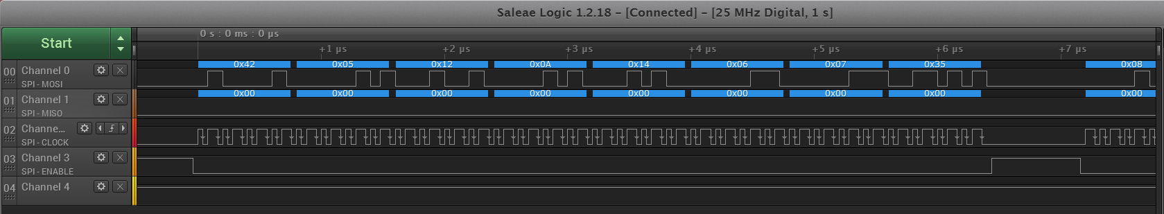
SSIDataPut(SSI0_BASE, 0x42);
SSIDataPut(SSI0_BASE, 0x05);
SSIDataPut(SSI0_BASE, RTD_CH1_INPUTMUX);
SSIDataPut(SSI0_BASE, RTD_PGA);
SSIDataPut(SSI0_BASE, RTD_DATARATE);
SSIDataPut(SSI0_BASE, RTD_REF);
SSIDataPut(SSI0_BASE, RTD_IDACMAG);
SSIDataPut(SSI0_BASE, RTD_CH1_IDACMUX);
while(SSIBusy(SSI0_BASE)){} // Wait until SSI0 is done transferring all the data in the transmit FIFO.
// Empty the garbage data in receive FIFO
SSIDataGet(SSI0_BASE, &dataRx);
SSIDataGet(SSI0_BASE, &dataRx);
SSIDataPut(SSI0_BASE, RTD_START_COMMAND); // start the initial conversion
while(SSIBusy(SSI0_BASE)){}
// Empty the garbage data in receive FIFO
SSIDataGet(SSI0_BASE, &dataRx);
}
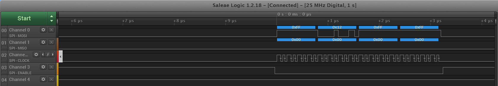
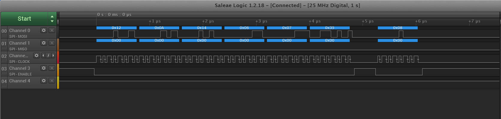
The picture below is from our logic analyzer. As clearly seen although master sends the data the slave always sends 0x00. Well, initially I thought this is garbage data so I can ignore it knowing the fact that I should empty my receive FIFO anyhow. For that I executed SSIDataGet twice as it can be seen above to empty receive FIFO (Note: here I assumed SSIDataGet function will empty two FIFOs by reading 32 bits, pelase correct me if I am wrong). But, when I executed only the first one the function started waiting. Well, we expect this if receive FIFO is empty so that I checked SSI_SR_RNE register and realized that it stays always zero even after executing the SSIDataPut eight times. It sounds the receive FIFO does not get anything from the slave.
Well, I ignored that and executed the following part in the main loop to read data from the slave:
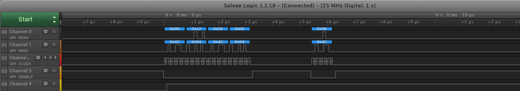
SSIDataPut(SSI0_BASE, Dummy_word);
SSIDataPut(SSI0_BASE, RTD_RDATA_COMMAND); // SPI (RTD_RDATA_COMMAND) data to request AIN1 - AIN2 value from ADS114S08
SSIDataPut(SSI0_BASE, Dummy_word);
SSIDataPut(SSI0_BASE, Dummy_word);
while(SSIBusy(SSI0_BASE)){} // Wait until SSI0 is done transferring all the data in the transmit FIFO.
SSIDataGet(SSI0_BASE, &dataRx);
result = dataRx & 0xFFFF; // Capture the the least significant 16-bit data after the second reading.
I executed SSIDataPut four times hoping that last receive FIFO register will have valid data so that I can easily read it. After evaluating the read data I execute the following part for next reading
// Start the conversion for next reading
SSIDataPut(SSI0_BASE, RTD_START_COMMAND);
while(SSIBusy(SSI0_BASE)){}
SSIDataGet(SSI0_BASE, &dataRx); // Ignore the result
As it can be seen, the last 16 bit is always zero which does not make sense to me. I also attached the picture of my setup. Any advice on this problem? Thanks in advance...