This thread has been locked.

If you have a related question, please click the "Ask a related question" button in the top right corner. The newly created question will be automatically linked to this question.

ADS131A04: ADS131A04 READY / SPI Communication

Part Number: ADS131A04

Hi,

I realized a prototype includeing the ADC ADS131A04. The pins M0, M1 and M2 are condigured as folowing: M0 = HIGH, M1 = HIGH, M2 = LOW. Thus Hamming Code Word validation is off, the ADC is operated in asynchronous interrupt mode with a SPI transfere word size of 32 Bit.

I'm initializing the ADC as suggest in section 10.4 (page 78).

  1. ADC Power is turned off. 
  2. The pins M0, M1 and M2 are set by resistors (500 Ohm) to the levels mentioned above (M0 = HIGH, M1 = HIGH, M2 = LOW).
  3. Enabling the external master clock (16 MHz, CMOS).
  4. ADC power is turned on (V_ADD = 3.3V; V_IOVDD = 3.3V)
  5. ADC !RESET! pin level is set HIGH
  6. A software RESET is performed to check if ADC is ready, by outputting 0xFF04

The SPI interface is operating in Mode 1, with a frequency of 2 MHz (according to the logic analyzer).

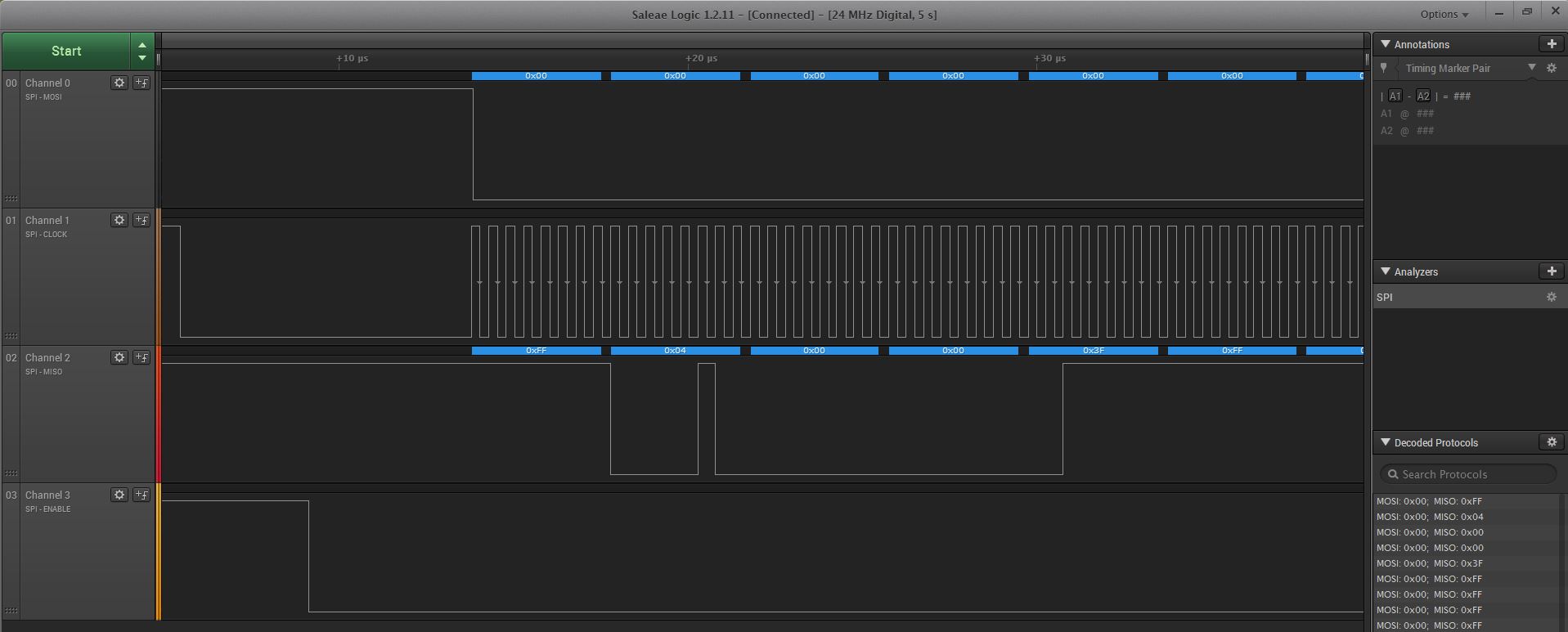
The following image shows the data captured by a logic analyzer, for a Software Reset (0x0011).

As can be seen, the ADC STATUS RESPONSE starts with 0xFF04, indicating the ADC is ready. But I would expect a further READY (0xFF04) response after several SPI cloclcks / Data Frames, as indicated in section 9.5.3.2 (page 50). I clocked in/out 8 Data Frames (each consisting of 32 Bit). The first 32 Bit is 0x00110000, the remaining Commands are the NULL command (0x00).

I also performed a "stand-alone" NULL command (section 9.5.3.1 on page 50).

As can be seen, the Status Response results in the expected response 0xFF04. The ADC is in LOCK - State, so I'm curious which ADC register content is clocked out, as a response of the NULL command. See second data frame in figure 68.


I'm a little bit confused by the read register states. According to section 9.5.3.5 on page 51, the UNLOCK, NULL, RREG, and RREGS commands are the only commands that are
recognized when reading back data in LOCK state.So I also perforemed a read command of register 0x05. Which also results in the same response, as the shown in the two previous images.

Maybe I read over some important part in the datasheet. Is there an additional High/Low transition required after a Data Frame?

BR

  • Hello Stenzer,

    Thank you for your post.

    Let me clarify a couple things to get started. First, as you found, there are only four commands that can be sent while the device is in a locked state upon power-up: UNLOCK, NULL, RREG, and RREGS. The RESET command (0011h) cannot be used during the initial power-up sequence.

    Second, the beginning and end of a frame is only marked by a transition on /CS. Each word in the frame must consist of the number of bits specified by the M1 setting. The device powers up in Dynamic-Frame Mode with CRC disabled, so the first frame only needs to consist of one, 32-bit word.

    The Command Status Response is located in the first word in the next frame (i.e. after /CS is taken high and returned low). The response to the NULL command will always be the register contents in the STAT_1 register.

    Please let me know if you have any further questions.

    Best Regards,

  • Hi Ryan,

    thank you for your reply. The /CS transition was missing. According to section 9.5.2.1.1

    Chip select (CS) is an active-low input that selects the device for SPI communication and controls the beginning and end of a data frame in asynchronous interrupt mode. CS must remain low for the entire duration of the serial communication to complete a command or data readback.

    This was a little missleading :D.

    I performed a SPI communication consisting of an UNLOCK Command (0x0655), a single register read RREG of register 0x0C (-> 0x2C) followed by a NULL command (0x00). The result without a /CS transition at the end of the Data Frame can be seen here:

    As can be seen, the result doesn't looks as hoped-for (0xFF04; 0x0655; 0x2C3C).

    The correct result determined by an additional /CS transition at the end of a Data Frame can be seen here:

    The correct MISO readings can be seen in the right lower corner, resulting in 0xFF04; 0x0655; 0x2C3C. Where 0x3C (of the last Data Frame) is the default register setting of register 0x0C (wgich is read by the command 0x2C).

    Ryan, thank you very much!!

    BR stenzer

  • Hi Stenzer - I'm glad you got it to work!

    Regards,