This thread has been locked.
If you have a related question, please click the "Ask a related question" button in the top right corner. The newly created question will be automatically linked to this question.
Hello all,
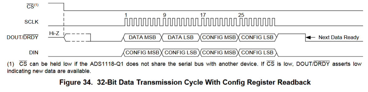
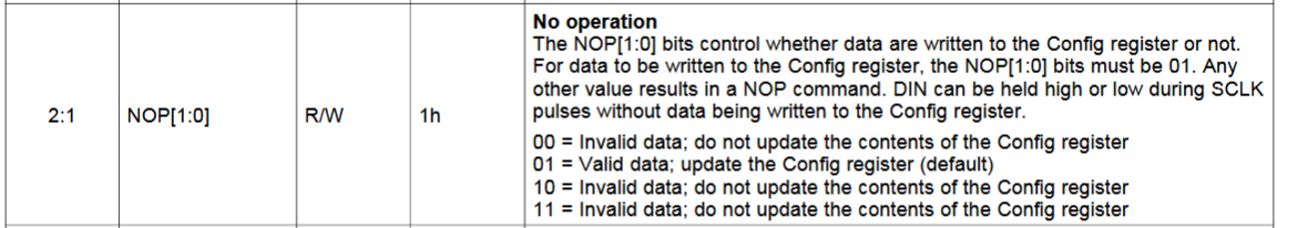
Thank you for your support always. I have a question about what happens when the 1st-and-2nd-byte and 3rd-and-4th SPI input on DIN are different.
In the datasheet, the 1-2 bytes are CONFIG MSB/LSB and 3-4 bytes should be those registers again or all L or all H. However, the IC can receive different bytes because of programming bug/noise or anything. Can you tell me what happens when something is happened?
Thank you,
RYO
RYO,
I believe what you're asking about refers to Figure 34 in the datasheet with the 32-bit transmission cycle with configuration register readback. I've a attached a picture below:
The configuration register is two bytes. In Figure 34, when you write to DIN, you want to write the two bytes to DIN and then write the same two bytes to DIN again.
If bytes 1 and 2 do not match bytes 3 and 4, the device will take bytes 3 and 4 for the data to write into the configuration register if this data is a valid write.
In the Configuration Register on page 24 you can see that bits 2:1 may act as a NOP. If these bits are 00, 11, or 10, then this write to the Configuration Register is ignored. This way a write of all 0s or all 1s to the register is ignored.
If these bits are 01, then the command is valid, and the data are written to the configuration register.
Hopefully, this answers your question. If you have more questions on the ADS1118, or if I didn't answer your original question, please post back.
Joseph Wu