This thread has been locked.

If you have a related question, please click the "Ask a related question" button in the top right corner. The newly created question will be automatically linked to this question.

ADS1158: Problems with exceeding range of the ADS1158

Part Number: ADS1158
Other Parts Discussed in Thread: REF5040, OPA365


Hello everyone,

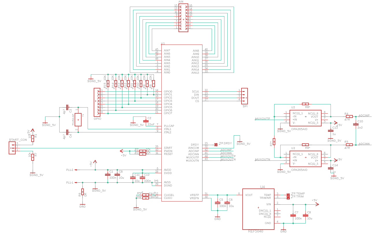
I have a problem with the ADS1158.

I have the circuit as shown in the picture built and put into operation. 5V supply voltage. (CLKSEL is connected to GND.)

Approximately 35mA current consumption. 2.5V reference voltage. The quartz works without distortion.

I can configure the ADC as desired, but unfortunately when I read its registers, I get in response:

Over voltage Protection, and the maximum value, or the minimum value as output voltage.

Over all Channels the same result.

I tried it with the differential measurement between two channels -> still max or min value.

Then I connected AINCOM to GND. Didn´t do anything.

I already played a little bit around with the AVDD and the VREF and START but without any success.

Afterwards I connected ADCINP to 2.5V and ADCINN to GND.

Still these answers...:

Config results: a 0 0 0 1 0 35 fe 80 9b
RX: 0xfd 0x7f 0xff
RX: 0xfc 0x7f 0xff
RX: 0xf8 0x7f 0xff
RX: 0xfd 0x7f 0xff
RX: 0xfa 0x7f 0xff
RX: 0xf8 0x7f 0xff
RX: 0xfd 0x7f 0xff
RX: 0xfa 0x7f 0xff
RX: 0xe8 0x7f 0xff
RX: 0xfc 0x7f 0xff
RX: 0xfa 0x7f 0xff
RX: 0xe8 0x7f 0xff
RX: 0xfc 0x7f 0xff
RX: 0xf8 0x7f 0xff
RX: 0xfd 0x7f 0xff
RX: 0xfc 0x7f 0xff
RX: 0xf8 0x7f 0xff
RX: 0xfd 0x7f 0xff
RX: 0xfa 0x7f 0xff
RX: 0xf8 0x7f 0xff
RX: 0xfd 0x7f 0xff
RX: 0xfa 0x7f 0xff
RX: 0xe8 0x7f 0xff

Config Results is the result of the: "Read config command", which reads the first 10 registers.

RX values represent bytes 1-3 of a "Channel Data Read Command"

I don´t think that this is a software issue...

Is it necessary to connect ADCINP ADCINN MUXOUTP and MUXOUTN together with a OPAMP as Buffer?

Thank you for your fast respond 

(Used Microcontroller: ESP32)

  • Hi user 5772542,

    Welcome to the TI E2E Forums!

    I see you also posted this same question here: e2e.ti.com/.../716205.
    Did you encounter any issues with E2E when creating this thread? If so, please let me know... I'd appreciate any feedback that might help improve the E2E experience!


    Regarding your question...

    I would first recommend configuring the ADS1158 into fixed-channel mode so that you can try to validate the ADC's conversion results on a single-channel.

    As for the OVF and SUPPLY flags in the STATUS byte, what is your supply and reference voltage, and have you tried measuring them on a DMM to verify? These flags would seem to indicate that the VREFP/VREFN and AVDD/AVSS voltages are low. Make sure you provide supply decoupling capacitors between AVDD/AVSS and DVDD/DGND. Perhaps, these voltages are drooping due to missing decoupling capacitors, or in the case of the LDO reference, the reference voltage may not be stable without a capacitive load.

    Additionally, It seems like you may not be reading the ADC data fast enough, since the STATUS byte indicates that you are missing channels from time to time. This might also indicate that you are reading data while the /DRDY pin is going low, which may cause data corruption (the data is provided though an output shift register and you should avoid reading data while this register is updating). If you can, use the /DRDY pin as an interrupt to your MCU to help facilitate when you read the data.


    Best regards,
    Chris
  • Hi Chris,

    I am a colleague of the thread-creator.

    Thanks a lot for your fast reply, we really appreciate it!

    Christopher Hall said:

    I would first recommend configuring the ADS1158 into fixed-channel mode so that you can try to validate the ADC's conversion results on a single-channel.


    We tried several options here (fixed-channel and auto-scan, single-ended and differential), but with no noticeable effect. But we will proceed with the fixed-channel mode for the next tests.

    Christopher Hall said:

    As for the OVF and SUPPLY flags in the STATUS byte, what is your supply and reference voltage, and have you tried measuring them on a DMM to verify? 


    As mentioned, supply voltage is 5V and reference voltage is 2.5V. We played around with the voltages a bit and made sure they are stable.

    Christopher Hall said:

    Make sure you provide supply decoupling capacitors between AVDD/AVSS and DVDD/DGND. Perhaps, these voltages are drooping due to missing decoupling capacitors, or in the case of the LDO reference, the reference voltage may not be stable without a capacitive load 


    In fact we were missing suitable capacitors here. As far as possible we still tried to incorporate them in our test board and again we didn't see any changes. In general I doubt that the result we are getting can be explained only with missing capacitors. the voltages are quite stable (when looked at with an oscilloscope). But we will take more care on that with the next design.

    Christopher Hall said:

    Additionally, It seems like you may not be reading the ADC data fast enough, since the STATUS byte indicates that you are missing channels from time to time


    That is true, we are reading with just 10 Hz currently (no specific reason, mainly to not spam the monitor). We will increase the poll rate significantly once the device is working as expected. The low data rate should not make any difference to our problem, right?

    Christopher Hall said:

    This might also indicate that you are reading data while the /DRDY pin is going low, which may cause data corruption (the data is provided though an output shift register and you should avoid reading data while this register is updating). If you can, use the /DRDY pin as an interrupt to your MCU to help facilitate when you read the data.


    We are not using the ADS1158 in direct read mode but in "register format" (Channel Data Read Command). According to the datasheet, we do not need to monitor DRDY in this case. Furthermore, it seems that the data we read from the device makes sense (status and data bytes are semantically coherent).

    Currently we have no circuit on ADCINN/P or MUXOUTN/P. Is it necessary to implement the recommended OPA-circuit? As far as we understood, the ADC should still be able to operate without any external circuitry here.

    Thanks a lot for your help!

  • Hi Chris,

    I am an other colleague of the tread creator.

    Today we have improved our schematic design of the Testboard for testing the ADS1158. We would be very glad, when you give us some input, commentary, recommendations, confirmation or otherwise before we start to assemble the next test circuit board.

    The common power supply of the board is 5V. The components, which marked with '*' are assembly options for better testing. 

    Additional to the previous version we included OPAMP buffer, a lot of coupling capacitors and REF5040 as voltage reference with a separate ground trace.  We connected pull-down resistors to all GPIOs for the unconnected State.

    When we take the REF504 the voltage of the analog inputs have to be lower than 4,096V x 1,06. It this right?

    The start-pin can be controlled by the microcontroller or alternative it can be connected to +5V or ground. The DRDV-Pin get a testpoint, when we need later the additional option of it.   

    Thanks a lot for your support!

  • Hi Felix, Hi Silke,


    Currently we have no circuit on ADCINN/P or MUXOUTN/P. Is it necessary to implement the recommended OPA-circuit? As far as we understood, the ADC should still be able to operate without any external circuitry here.

    You are correct, you can use the internal MUX to measure the inputs directly without having to routing the signal through the MUXOUT and ADCIN pins.

    However,  note that the ADC inputs do directly into an unbuffered switched-capacitor input. If your signal sources are not buffered or if they have a significant output impedance you'll find that connecting directly into the ADC will result in large gain errors. Therefore I generally recommend adding external buffers between the MUXOUT and ADCIN pins.


    Silke Allebrod said:
    Additional to the previous version we included OPAMP buffer, a lot of coupling capacitors and REF5040 as voltage reference with a separate ground trace.  We connected pull-down resistors to all GPIOs for the unconnected State.

    I think these are all good changes....One thing you still need to consider is if the op-amp circuit's linear output range will be sufficient for the input signals you are planning to measure.  The OPA365's outputs can drive to within 200 mV of the supply rails before beginning to saturate. Therefore, if any of your inputs signals are close to 0 or 5V, or if the differential input voltage gained up by the OPA365's, would results in either op-amp's output approaching 0 or 5V, then you'll run into linearity issues.

    So that begs the question, what are the input voltages you are planning to measure? If they are singled-ended, then you may want to measure them with respect to some mid-supply voltage, for example, by connecting AINCOM 2.5V and measuring the differential voltage between AIN0 and AINCOM.

    The only additional changes I would suggest are:

      • Consider using a single ground plane (see my question/comments below).
      • Consider adding a capacitor to the REF5040's TRIM/NR pin to provide additional reference noise filtering.

      • Consider using a crystal oscillator instead of an external crystal connected to the ADS1158. Should you decide to stick with a crystal, you'll need to do some additional testing to ensure that the crystal starts-up without any issues over temperature. If you search E2E, you'll notice that crystal start up issues are quite common with the ADS1x58 and many 32.7 kHz crystals. Using a crystal oscillator (integrated crystal + crystal driver circuit) is usually a safer option since the crystal oscillator manufacturer has done the work to ensure crystal and driver circuits are compatible and work well together over temperature.

      • Finally, if your SPI signals are being jumper wired to another PCB with your MCU, then consider adding another pin to your SPI header that connects to ground. You'll want to keep your SPI signal wires short and also have a nearby ground wire to reduce the loop area between signal and ground (hence improving signal integrity).


    Silke Allebrod said:
    When we take the REF504 the voltage of the analog inputs have to be lower than 4,096V x 1,06. It this right?

    Correct, the differential voltage between any two inputs (which you select) must not exceed  4.096 V * 1.066... or ~4.36V. This requirement is in addition to the common-mode range limitations of the OPA365 circuit you've created.


    One observation I had on the schematic is that you use two different ground plane nets. Is there a reason why you need to do this in your design?

    Generally, I discourage the use of split ground planes with precision ADCs...the analog and digital ground pins of the ADS1158 need to be connected together, preferably as close as possible to reduce common ground impedance between these grounds.

    One major problem with split ground planes is that it often leads to traces being routed over gaps in the ground plane, which in turn inhibits the flow of return current below these traces and make the traces much more inductive. If you stick with separate grounds, make sure you short them below the ADC and do not route traces over any ground plane gaps or cutouts.


    Best regards,
    Chris