This thread has been locked.

If you have a related question, please click the "Ask a related question" button in the top right corner. The newly created question will be automatically linked to this question.

ADS1231: Data is never READY

Part Number: ADS1231

Hi to all,

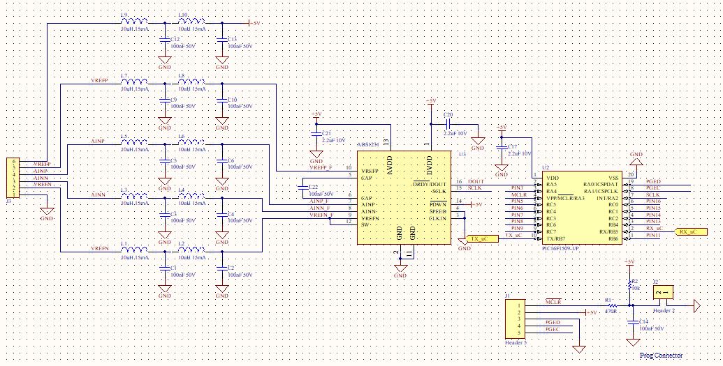
I'm trying to read a cell load with the ADS1231. I'm using the same circuit of page 16.

I connected the cell load and power on the circuit but the pin DRDYn/DOUT never goes down so that no conversion starts.

I checked all the connections and voltage on eache pin of ADS1231.

Am I wrong something else?

Thank you for your support

  • Hi Serafino,

    Make sure the PDWN pin is high otherwise the device is in a powered down state. Also make sure that you are using Mode 1 SPI where SCLK idles in a low state, and data is changed on the rising edge of SCLK and data is read on the falling edge of SCLK. If SCLK is high, then the ADS1231 will be in standby mode and no conversions will take place.

    If the device is operating normally, then you should see pulses on the DRDY/DOUT pin at the period of the selected SPEED pin setting. For SPEED pin low (0) the DRDY/DOUT should pulse approximately ever 100ms, and with SPEED pin high (1) the pulse occurs approximately ever 12.5ms.

    Best regards,
    Bob B
  • Hi Bob,

    thank you for your reply.

    I yet checked that the PDWN is high (+5V) and SCLK is low.

    But nothing happens: the DOUT is always high.

    Best regards

  • Hi Serafino,

    If both the analog and digital supplies are working and the PDWN and SCLK are correct, I would double check the connections to the micro to make sure you are not driving the wrong pins.  This is a very simple part and there is not much that can go wrong.

    Can you send me a picture or 2 of your setup?

    Best regards,

    Bob B

  • Dear Bob, thank you for your support.

    Here below the electrical scheme I'm using

    And here below the top and bottom of the PCB

    Here below the PCB

    I tried to exchange the IC but nothing changes.

    If you note something wrong, please tell me.

    Thank you for your support

  • In the datasheet it is mentioned that the DOUT signal goes down when a "valid data" i available: what means as "valid data"?
  • Hi Serafino,

    There are a number of general comments I can make regarding your circuit and PCB layout, but let's start with the issue with DRDY\DOUT. Valid data refers to the conversion has completed and the results read from the ADS1231 are correct for the input to the device. If you attempt to read data while DRDY\DOUT is high, the data is invalid for the conversion that is in process.

    As far as DRDY\DOUT never going low, this may be due to your device configuration. If you look at Figure 22 on page 15 of the ADS1231 datasheet, you will notice that PDWN must stay low for at least 10us after AVDD and DVDD are at the nominal voltage. In your schematic you show PDWN tied high to the supply. The ADS1231 requires that for proper startup, the PDWN pin should remain low for the required amount of time. The best way to accomplish this task is to use a GPIO on the micro to hold the pin low until the proper time has elapsed. Also, you can reset the device by pulsing the PDWN pin from the micro.

    Regarding your circuit, you use a lot of ferrites as pi type networks but no resistors. To create a good anti-aliasing filter you should use a resistor in your analog input path. For example replace L4 and L6 with resistors. C4 and C6 are quite large so you may want to reduce them if you use resistors. You should also have a differential cap between the analog inputs that is 10x larger in value than the common-mode caps (C4 and C6).

    To help reduce overall noise, it is best to use a ground plane area as opposed to just ground traces.

    I would suggest fixing the PDWN pin first, then analyze your data. Implement other changes as needed to correct any other possible issues mentioned above.

    Best regards,
    Bob B