This thread has been locked.

If you have a related question, please click the "Ask a related question" button in the top right corner. The newly created question will be automatically linked to this question.

ADS131E08EVM-PDK: Input Seems Attenuated by a Factor of 2 and VREFP Doesn't Seem to be Supplied Internally

Part Number: ADS131E08EVM-PDK
Other Parts Discussed in Thread: ADS131E08

I am trying to develop a demo using the ADS131E08EVM-PDK and am noticing that the input seems to be attenuated by a factor of 2. I am also noticing that VREFP doesn't seem to be supplied internally. I think this may be because I am not using the Modular EVM Motherboard and am instead using Test Points 7 and 10 to power the board, so if this setup will cause damage to the board, please let me know.

I am using an NI PXIe-4145 to power the board by supplying 5V to TP 7, supplying one power supply low to TP 8 (all power supply grounds are tied internally and are floating), and I am supplying 3.3V to TP 10. To work around the VREFP behavior and some unstable behavior on VREFN, I've supplied 2.5V to TP 3 and -2.5V to TP6 (because AVSS is tied to VREFN). I am also using an NI PXIe-4463 to generate a sine wave (±2.5V) and am feeding it into channel 1 of the EVM. Finally, to acquire the data, I am using an NI PXIe-6570 and am acquring data on the SPI lines. I've attached an image below of my wiring (please forgive the clutter) as well as a simplified image to show which test points and pin headers are being used.

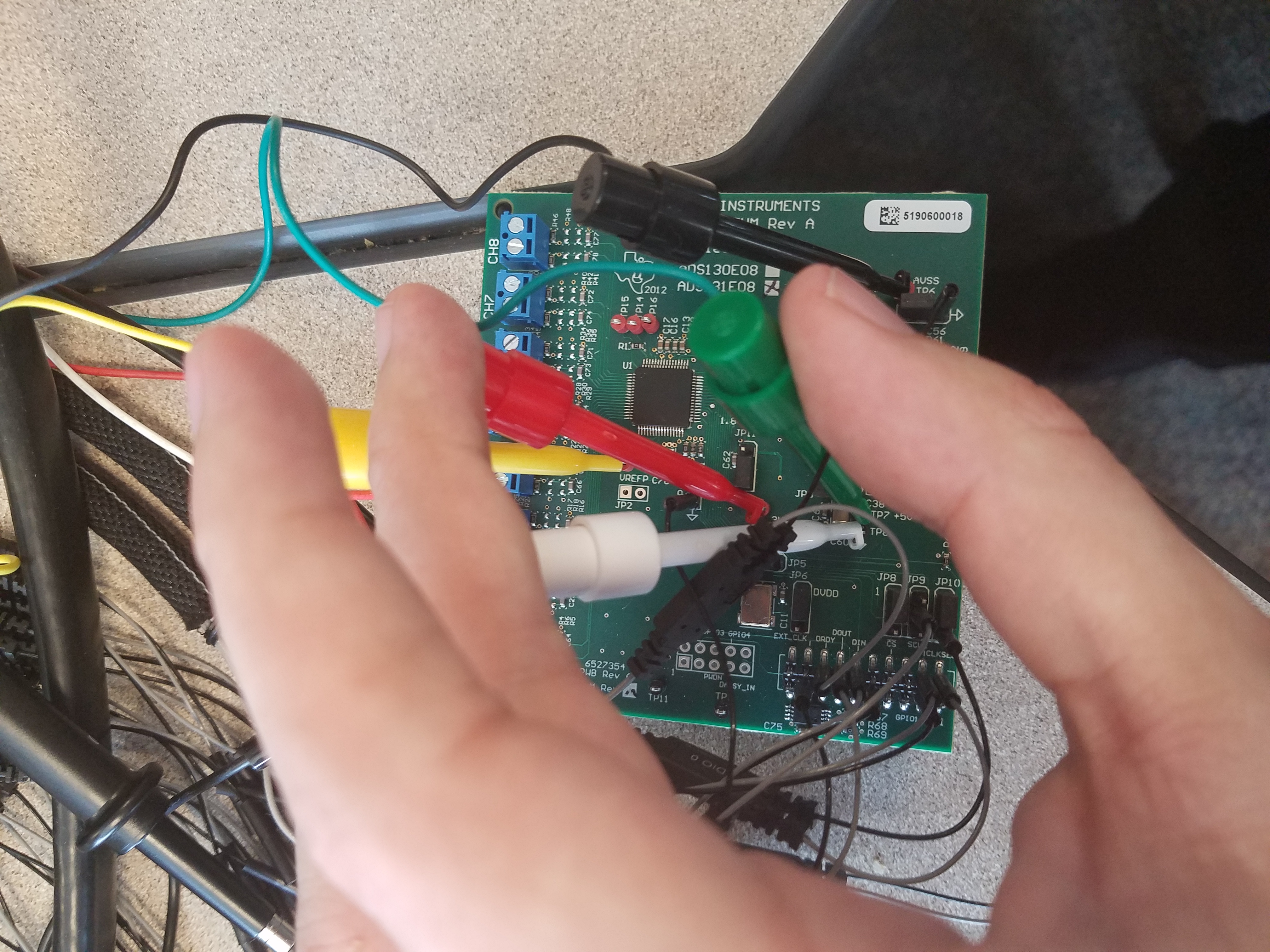
(Pin 2 on the J1 header isn't used, I simply labeled it to make it easier to understand the numbering convention)

The reason I believe the signal supplied is attenuated is because when I feed in a sine wave with an amplitude of 2.5V, the data I receive back scales to a 1.25V sine wave. I've double-checked the signal fed in by supplying a constant 1V and reading back 1V on a DMM. When I read the same signal from the ADC, it's scaled as 0.5V. Also, when I read the raw ADC binary for the 2.5V amplitude sine wave, there is a gap in codes between ~16000 and ~44000, indicating that the signal being read is roughly half of the full scale range.

Finally, one major concern I've had is that after performing constant testing on one ADC, the THD fell out of specification, which made me think I may have damaged the part. I haven't seen the THD fall on a second ADC after minimal testing, but since I briefly saw the correct amplitude read back on the second ADC and then saw it read back an attenuated value about 15 minutes later, I was concerned I was causing damage to the part.

All of that said, I have a few questions:

  1. Is the setup without the motherboard causing damage to the EVM?
  2. If the answer to (1) is no, is the motherboard supposed to supply the VREFP internal voltage, and if it is, would it damage the EVM to supply this externally via TP 3?
  3. If the board isn't being damaged, is there a reason why the signal seems to be attenuated?
  4. If I must use the motherboard, can I still communicate with the EVM via SPI?
  5. Not related to problematic behavior, but one thing I was wishing to demonstrate was INL testing. Do you perform the histogram INL method for your tests, or do you use a different method?

If there is any information that is missing, please let me know, and I'll supply whatever I can!

  • Hello Jonathan,

    Thank you for your post and welcome to our forum! I appreciate the amount of detail you've provided as well.

    For starters, I have a few clarification comments and questions regarding your setup:

    1. How are the jumpers JP1 and JP7 configured? The center of each jumper (pin 2) is connected to AVDD and AVSS, respectively. You might have an issue where the outputs of U6, U7, or U8 are trying to driving the test points which you have connected to external supplies (see page 38 of the User Guide). If you are supplying 5 V to TP7, then you can use JP1 and JP7 to select the appropriate analog supply for the ADC.
    2. What are the register settings that you are writing to the ADC? You must write to the CONFIG3 register to enable the internal reference buffer. Please specify the complete list of register settings used to configure the ADS131E08.
    3. The digital supply (DVDD) must be provided as you have done (TP10 = 3.3 V and JP11 = [2-3]).
    4. How are you applying the input signal: single-ended or differentially?

    If 5 V and the desired DVDD voltage (i.e. 3.3 V) are provided to the EVM, you should be able to use it without the MMB0 and without damaging the device. Just be mindful of how the jumpers are configured and ensure that multiple sources are not driving the same supply rail.

    Let me know if the data looks the same after you've fixed the supply connections and enabled the internal reference voltage. If you can, please share a screen capture of the Scope tab displaying the data and the list of register settings.

    Best Regards,

  • Thank you for your response, Ryan!

    I've read through this and talked with a local FAE, and I have some updates for this post. I'll start off by answering your questions above then go into the other information I have.

    1. JP1 and JP7 are both configured to jumper the left and middle pins together.
    2. I was not writing to CONFIG3 register and instead trying to use the device in its power-up state. I will write to the register and probe TP3 to verify that VREFP is being supplied internally.
    3. Yes, the digital portion of the device seems to be working as expected.
    4. The signal was being supplied single-ended, and after talking with the FAE, I realize that I was misinterpreting FS range (I was reading it as highest positive and negative value with respect to zero, not with respect to the other reference).

    My plan today is to write to CONFIG3 to enable the internal reference buffer, probe on VREFP to verify that the voltage reference positive is being supplied properly, and try altering my software/hardware setup to supply a differential signal and verify that my "attenuation" was actually me losing 3dB by supplying a single-ended signal.

    After I finish those steps, I'll update this post with what I find. Thank you again for your help!

    Regards,

    Jonathan (Andy) Freberg

  • Hello Jonathan,

    My point about the analog supplies was that you do not need to provide an external supply for AVDD or AVSS as long as 5 V is provided to TP7. The LDOs (U6-8) will generate the necessary supplies. Simply configure JP1 and JP7 as needed for unipolar or bipolar supply operation.

    Note: if both jumpers are to the left (i.e. [2-3] position), then this violates the analog supply range since AVDD = 3 V and AVSS = -2.5 V. The max difference between AVDD and AVSS is 5.25 V. Please use the Recommended Operating Conditions table as a guide for device restrictions, not the Absolute Maximum Ratings table.

    Best Regards,

  • HI Ryan,

    I've performed the following troubleshooting steps based on your suggestions:

    1. Verified that JP1 is configured 1-2 and that JP7 is configured 2-3 (they are)
    2. Sent the following SPI commands in order after powering on the ADS131E08:
      1. 0x11 (stop read data continuous)
      2. 0x43 (write register 3)
      3. 0x00 (write to 1 register)
      4. Here I've tried a few different commands to see if any of them have worked (none have so far)
        1. 0xC0 (enable internal reference buffer)
        2. 0xC4 (same as above, but also enable op amp)
        3. 0xCC (same as both above, but also connect the non-inverting input to [AVDD +AVSS] / 2)
      5. 0x10 (start read data continuous)
      6. Burst pattern to read continuous data (I know this portion is working)

    3. Probed VREFP after sending those SPI commands both with an SMU and with a DMM (after disconnecting the SMU) by connecting positive probe to TP3 and negative probe to board ground (SMU using TP8, DMM using TP11).
      1. The value came out to -0.08 V, which is different from the -2.3 V I was reading before, but still not the 2.5 V I'd expect.
    4. I verified that the SPI commands were being read properly by skipping the start read data continuous command and noticed that the board output all zeros after the first read. When I re-enabled the start read data continuous, the board was giving expected outputs. I also read back CONFIG3 where I'd set the register to "C0" and read back "C1" (which seems expected since the note on bit 0 was "will return either 0 or 1")

    My outstanding questions are as follows:

    1. Why does VREFP not seem to be supplied internally given the above configurations? (J1 = 1-2, J7 = 2-3, CONFIG3 = C0)
    2. Are there any other registers/jumpers that need to be configured in order to supply voltage properly to VREFP?

    I'm at a loss on what to do next, so any advice is appreciated!

  • Hi Jonathan,

    Remember that the analog voltages on the ADS131E08 are all with respect to AVSS, not ground. JP1 and JP7 are configured for bipolar supply operation (AVDD = 2.5 V and AVSS = -2.5 V) according to your last post. Therefore, I expect the voltage on VREFP to be 2.4 V above AVSS, i.e. -100 mV. There may be a slight error due to the DMM leads or some noise on the ground, but if you probe directly across VREFP and VREFN, it should be close to 2.4 V. We screen the internal reference voltage according to the min/max specs in the Electrical Characteristics table, so probing the pins should just be a sanity check.

    Best Regards,

  • Hi Jonathan,

    Did you get this figured out?

    Best Regards,