This thread has been locked.

If you have a related question, please click the "Ask a related question" button in the top right corner. The newly created question will be automatically linked to this question.

ADS5400: Maximum clock input to an unpowered device.

Part Number: ADS5400

I am trying to determine the maximum allowed clock input signal to an unpowered ADS5400. In other words, can a differential clock be applied prior to power on?

  • Hi Charles,

    We are taking a look into your question, and will be back with you soon.

    Best Regards,

    Dan
  • Hey Charles,

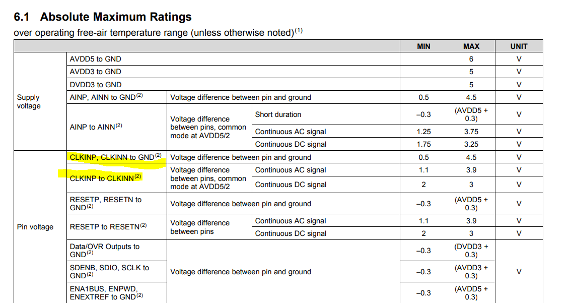
    Leaving the device powered down while applying a clock input will stress the ESD diodes. I dont think this will be detrimental unless the voltage surpasses the absolute max found in the datasheet.  Reference the following picture. 

    Yusuf

  • I had already examined the data sheet. The data sheet snapshot provided is not complete. The referenced Note 2 states under nominal supplied input voltage. If the ESD diodes are stressed that could alter the interface characteristics significantly and cause detrimental behavior. This is what I am attempting to understand. When discussing ESD damage it would not only include voltage but current capability as well.
  • Hey Charles,

    It does not matter if the device is turned on/off, if you're violating the absolute max spec of the device than you will permanently damage the device.

    Yusuf
  • The absolute maximum specifications do not address power off and do not make sense relative to a power off condition. For example, the specification states that the minimum of the clocks to gnd is 0.5 to 4.5. Obviously, with the device off and nothing driving it, this cannot be met. Most of the time, these specifications are written w.r.t. VDD itself. In the A/Ds case, they assume power is applied and within certain limits.

    Then there is the second requirement of the voltage DC between the two clock pins must be a minimum of 2V and maximum of 3V. I do not understand this one at all. The clock signals is driven with an AC coupled  balun. I would expect 0V DC between the pins.

    CLKINP, CLKINN to GND(2) Voltage difference between pin and ground 0.5 4.5 V

    Voltage difference Continuous AC signal 1.1 3.9 V

    CLKINP to CLKINN(2) between pins, common

    mode at AVDD5/2 Continuous DC signal 2 3 V

    Charles

  • Hey Charles,

    The specs in the datasheet were all derived while the device was powered on. Therefore, there is no way to definitely answer your question on max input signal when device is turned off or guarantee that the device will still operate within spec.

    Thanks

    Yusuf