This thread has been locked.

If you have a related question, please click the "Ask a related question" button in the top right corner. The newly created question will be automatically linked to this question.

ADS1258 low data rate SPI connection

Other Parts Discussed in Thread: ADS1258, ADCPRO

Hello,


I am trying to connect my ADS1258EVM board to a gumstix computer via SPI. I shifted the logical level to 3.3V and connected SCLK, DIN, DOUT and CS. Trying to poll the data i dont think i need any more, do i? START is pulled low, PWDN high.

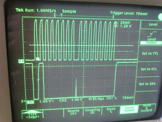
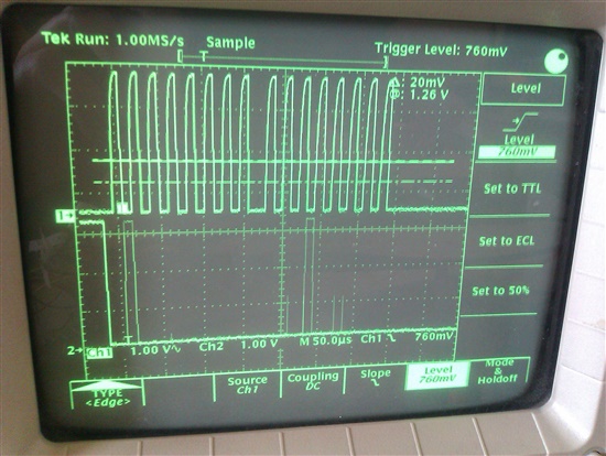
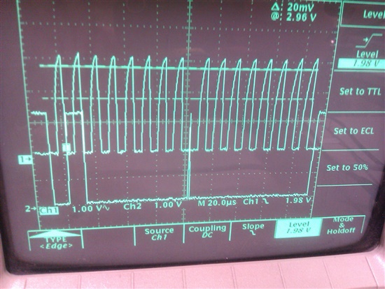
Well, after I did connect everything and i see the correct signal on the scope (unfortunately an analog one, so i cant really send you plots). I am only trying to read the ID Register first, so I send 0x4000 to the ADS1258 and read the second byte in my response buffer.

With a data rate 6400Hz I dont get any response (0x00). Increasing the data rate I get some results which look pretty much random. I cannot exceed the data rate further than approx. 100 000Hz because my level shifters are too slow. I am wondering if this can be a problem with the ADS1258.

I am pretty confident that the ADS1258 does not even understand my request, because i was also sending other commands (register write, data read, data read direct etc.) and only get back random data on DOUT. I am guessing that somehow i am triggering the device to send data, but i am not really sure why this misinterpretation happens.

I would appreciate if you could give me some hints, maybe also how i could debug this error, because i am running out of ideas.

Regards,

Norman


  • Norman, 

    The first place I would look at is the polarity and phase of the SCLK to DIN and DOUT. In the ADS1258, the data on the DIN line is latched into the converter on the rising edge of SCLK and changes on the falling edge. The DOUT is meant to be read out on the falling edge of SCLK. You state that you are reading out some data when you read back, however, the data appears to be random. It may be that you are using the wrong edge.

    The next thing I would do is look into reading back the CONFIG0 register by writing 0x40 and then reading back what appears on DOUT. You should read back 0x0A, the default reading.  

    Regards,

    Tony Calabria

  • Hi Tony,

    thanks for your first suggestions. My clock polarity anall seems fine. I set it up with SPI mode 0 which corresponds to what you describe i suppose.

    I took a pic of my scope and what i get trying to read the register CONFIG0.

    Top: SCLK, Bottom: DIN: 0x40:

    Top: SCLK, Bottom: DOUT with random data. What you cannot see in the image is that the data sent over DOUT changes all the time

    A short excerpt of the resulting data i get:

    Register 00 : 48
    Register 00 : 00
    Register 00 : 00
    Register 00 : 00
    Register 00 : 28
    Register 00 : 00
    Register 00 : 00
    Register 00 : 00
    Register 00 : 00
    Register 00 : 00
    Register 00 : 00

    What you might notice is that i have my transmission lines pulled high in idle phases. That is due to my level shifters and shouldnt cause problems, should it?


    What i notice now that i took the picture is, that the ADS1258 seems to clock on both, rising and falling edge....  What could be the reason for that?

    As i said in my first post im using the ADS1258EVM board. Could it be that i missed something setting that up?


    Regards,

    Norman


  • Hi Norman, 

    That is very interesting that the data on DOUT appears to be changing on both the rising edge and falling edge of SCLK. Have you made sure that you are applying all the necessary power signals to the J5A header. Powering just some of the power signals may be powering the ADC but not powering circuitry around the part. For example, if you look at U12 (voltage level translator) on the schematic, you can see that it requires both 3.3V and DVDD in order to make sure the SDI lines are attenuated to the proper level depending on the how ADC's digital circuitry is powered. If both those supplies are not powered, you will have issues in your communication. I would try probing the SPI signals at the pin of the ADC to see what the signal is that is getting to the part. You can also try idling your DIN, DOUT, SCLK signals low instead of high to see if that helps.

    We have software available for the ADS1258, where you can monitor our communication signals as an example. This may be the easiest way to see our timing and how we read and write to registers. All you need is a USB cord and the MMB0 motherboard. If you do not have a MMB0 motherboard, I can send you one for you to play with.  

    The software for the ADC evaluation is called ADCPro and is available at http://focus.ti.com/docs/toolsw/folders/print/adcpro.html

    The plugin of ADCPro for the ADS1258EVM is located at the product folder page: http://focus.ti.com/docs/toolsw/folders/print/ads1258evm-pdk.html

    Regards,

    Tony Calabria

  • Hi Tony,


    I have the MMB0 and worked a bit with ADCPro and also got really nice results with it. That is also the reason why i am sure the ADS1258EVM-Board works, no damage on the hardware.

    Well, but now i want to get rid of the PC software and measure outside, so i need my connection to the embedded computer.

    Concerning  power supply, i have connected +5VA to 5V, -5VA to GND, DGND to GND and 3.3V to 3.3V, all on J5A. On Jumper J4 i set everything up the way it is described in the manual. So DVDD should also be connected to the 3.3V on the J5A, right? And as you can see, the level of the data that is sent out is 3.3V level....

    I now also probed the pin at the ADC directly before U12, and it looks just fine (dont be irritated by the SCLK-signal that is a bit messy, directly at the pin of the ADC it looks perfectly rectangular, the mess is due to my level shifter and the level shifter on the ADS1258EVM fixes it i suppose):

    Some other tests i did today were checking the DRDY-pin, which gives me interrupts, but just as random as the data that is shifted out. My theory now is that the ADC also interprets the data on rising and falling edge and because there is no 100% defined state there sometimes gets a trigger to send data (maybe the pulse convert command?).

    So the basic question is: How do i get the device to trigger only on rising edge? Or: what could cause it to trigger on both edges?

    I really need to get that thing running, so i would appreciate any further help or suggestions....

    Regards,

    Norman


  • Hi again,

    something new i tried:

    I thought maybe level shifting is just not working, so why not try to connect the wires directly to the pins before they are shifted to 3.3V (setting the DVDD-jumper to 1.8V). Anyway all my signals ended up at 0.9V when i connected the gumstix and the ADS1258. Now i read in the datasheet that DVDD is min 2.7V and max 5.25V. So what is the jumper setting 1.8V for anyways then?? I dont get it...


    Still hoping for help...

    Norman

  • Norman, 

    Sorry for the delay, I have been caught up in a couple other things.

    The ADS1258 is designed to have the data output on DOUT to be read on the falling edge of SCLK. In the Figure 1 timing design, the DOUT bit is designed to change some tDOPD fixed time after a falling edge. So it is not necessarily true that the data changes on the rising edge. In essence, the data bit on DOUT actually changes some fixed time following a falling edge. So if you look at it on a scope using a slower SCLK, you may see that the data appears to be changing on the falling edge of SCLK. If you are to zoom in on it, you will see that it is, in fact, not changing on an edge but a fixed time following the falling edge of SCLK. The reason it is designed this way is so that the setup and hold times can be met of the ADC and uC when the SCLK is run at faster speeds. For that reason, the data should not be changing on both the rising and falling edge of SCLK. The only thing that I can think of is that is that something external to the ADC is driving the DOUT bit high or low in between SCLK periods.  

    As for the DVDD power supply, you are correct that it is specified to be 2.7V minimum, so I am not sure why we had put in the option to go as low as 1.8V. My thinking is that the EVM was being designed during the IC design period and the EVM designer was not entirely sure if the part would support 1.8V DVDD or not. Therefore, he added it in to be safe. Are you using the internal oscillator? and what SCLK speed are you using? 

    Regards,

    Tony Calabria 

  • Hi Tony,


    thanks for the answer. I am back to 3.3V with level shifters again... I also redid my whole wiring and all and now it looks like I read back correct data occasionally.... which is of course not sufficient really...

    Of course I now thought that maybe I have disturbances, perhaps should use termination on the data lines. What I really did is put a 100Ohm resistor and 100pF in series between the data lines and mass, which didnt help at all. Also the signal looks alright on the scope...

    So basically I am still puzzled what my key issue is here.

    To answer your questions: Yes, i am using the internal oscillator (32.768Hz, right?) and I tried various SCLK speeds as posted in my first post.  At those times when i did read correct data for some time i was running at 262.200Hz. I really cant go any higher because of my slow level shifters. What irritates me when I have a close look at figure 1 and table 1 is, that the minimum t_SCLK is 2*t_CLK, but I get best results (if any at all) with a t_SCLK that is far below 2*t_CLK.

    This could be something pretty simple but i dont see it yet.


    Regards,

    Norman

  • Norman,

    Enabling the internal oscillator will create a 15.729MHz master clock using internal PLL circuitry and the crystal oscillator. Looking at Table 1, tSCLK limit is 2 tclk minimum. This means that the minimum time that the SCLK period can be is 2 master clock periods. For example, if the master clock is 16MHz, the max SCLK is 8MHz. You are not exceeding this spec by using a 200Hz clock.

    Where you need to look is the tSPW spec, SCLK high or Low Pulse Width. If you exceed the maximum 4096tclk (256tclk if register bit set) then the SPI interface will reset. In order to stay within this spec to make sure your SPI interface does not reset, the minimum time that SCLK can be low or high is 521us limiting your SCLK to about 1.9KHz (assuming a 50% duty cycle).   

    (1/15.729e6) * (4096) * (2) = 521us. 1/521us = ~1.9KHz 

    Therefore, using a 252Hz SCLK, it looks like your SPI interface is getting reset every time SCLK is high or low as the high time and low time is exceeding the tSPW spec(high time/low time is 1.9ms assuming 50% duty cycle). You can try and use a slower external clock instead of the crystal to see if it helps. I have not tried this ADC using an external clock and SCLK rates as slow as 200Hz. In theory it should work if a slow external master clock is used. 

    Regards,

    Tony Calabria 

  • Hi Tony,


    i am not as low as 200 Hz, that was intercultural misunderstanding... im in germany and we use the dot like you use the comma. I am at 262kHz.

    In fact i managed to get my clock up to about 1MHz. My main problem now is EMC. A lot of my readings are just corrupt.

    That is probably something that you cannot really help me with, i just have to improve my connectors and wiring .

    Still your explanation of my scope images does not seem to apply, because if you look at the frequency i was clocking in that picture i posted, you see i am at 50kHz and the SCLK high or low pulse width is only 10u, and the DOUT also drops low again after 10us....

    I am not sure what was the reason there, it looks better now, so ... whatever...


    Thanks for your help

    Norman