This thread has been locked.

If you have a related question, please click the "Ask a related question" button in the top right corner. The newly created question will be automatically linked to this question.

TINA/Spice/ADS8900B: How to configure the front end with gain?

Part Number: ADS8900B
Other Parts Discussed in Thread: TINA-TI, OPA625, , OPA320, THS4551

Tool/software: TINA-TI or Spice Models

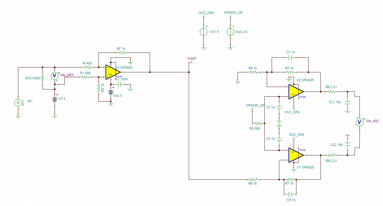
opa625_try.TSCI was tried to use the front end figure 105 shown in the datasheet of ADS8900B.

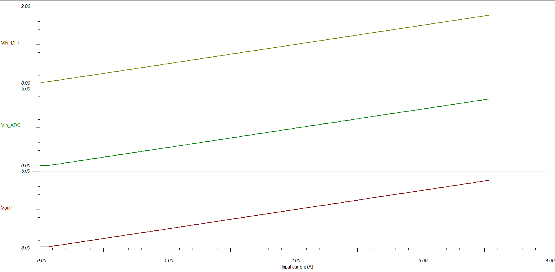
I need to measure the current from 0-3.5A in high side3.3V line in 10uA resolution. so that I chose this ADC[20-bit]. I am going to use 0.5Ohm current sense resistor and plan to measure by the drop of that resistor. I simulated this front end in Tina-TI as per the Figure i mentioned above. it gives very good response in the simulation and the changes for every 10uA also linearly changing in the simulation.

Since the reference voltage of ADC is starts from 2.5V, I need to map the resistor drop into full scale voltage, so I need gain amplifier. My input signal frequency may go upto MHz, so i need high bandwidth. so that i plan to use the same op-amp OPA625 For gain amplifier. I designed basing differential amplifier using this part and given the output to the front end of the ADC. the output is good but after few amperes say 50mA. This much initial amperes i cannot compromised. I need to avoid such limitations.

Can you please verify my design and suggest any modification?

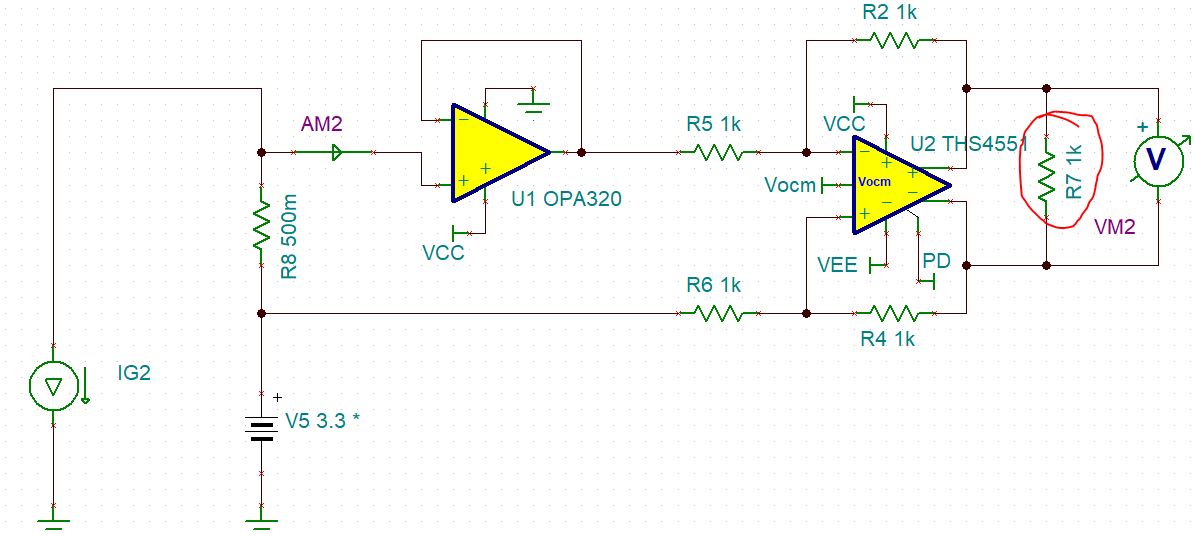
And I need to measure the current from 0-3.5A by 0.5A resistor (resistor drop range 0-1.75V). The full scale mentioned in datasheet is -Vref to +Vref but I need to map this resistor drop to this full scale value. Can you please suggest configuration tips? or can I use the configuration shown in the figure 111 in dataheet of ADC?

Here I attached the Tina Schematic design 

Output waveform(Notify initial few mA upto 50mA. the output is not started)

  • Hello,
    We are looking into this and will get back to you soon.
    In the mean time, it looks like you might be hitting an output swing limitation from the negative rail. The OPA625 has a 110mV limit from the rail. Would you confirm what voltage the OPA625 output is being limited to?
    Regards
    Cynthia
  • Hi Cynthia, Thanks for your response

    I thought to map the resistor drop voltage (0 - 1.75V) to the reference range 4.5V by increasing the gain to 2.5 V/V. So that I tried to design the circuit as instrumentation amplifier, which means i placed the gain amplifier section using opa625 is after the front end section. But that is not seems good in simulation itself. So I tried to place this amplifier section before the front end section. I realized that I am missing something but i don't know what exactly is.

    My design may be wrong approach or violating any limitation specified in datasheets.(full scale range, common mode voltage and Vref in ADS8900B). Can you please mention it and suggest appropriate design for the requirement I mentioned in the first question?

    At last I also think to design the front end suggested in the Tina-Ti reference design of ADA8900B (www.ti.com/.../toolssoftware) as it is and give the voltage drop across the resistor directly to this front end and Vref of ADS8900B is 2.5V. Will it be advisible?

    Regards,
    Venkatesh P
  • Hello Venkatesh,

    The ADS8900B requires a fully differential input to meet the common mode input spec.  Please see attached TINA-TI file for an example design using the OPA625.

    I also included a current shunt front-end amplifier to show how to bias it at 0.2V so you can use a single 5V supply and measure 0-3.5A input.

    Regarding the current shunt amplifier, you are proposing to use a 0.5ohm shunt resistor.  At 3.5A, this will result in almost 6W of power dissipation in the 0.5ohm shunt, and your load will see the 5V rail drop down to 3.25V.  Will either of these conditions be acceptable?  Usually for a current shunt, you want to limit the voltage drop to around 0.1V at max current, and keep power dissipation well below 1W.

    You may also be interested in the Analog Engineer's Circuits Cookbook.  The High Current Battery Monitor Circuit is very similar to what you want to measure.

    http://www.ti.com/lit/slyy138

    Regards,

    Keith N.

    ADS8900 Signal Chain with Current Shunt input V9.TSC

  • Hi Keith,

    Thanks for your valuable response.

    Average load current in my case is 500mA to 800mA so I have chose 500mOhm resistor so the effective dissipation is 320mW which is okey for me, the maximum current is occurs in rare and very few micro seconds so it may not be considered while resistor rating. And the line is 3.3V only. Sorry, I mentioned 5V in the previous post.

    I have chosen the figure shown in Figure 111 in datasheet of ADS8900B as you point out in our early discussion. I simulated it and it responses good.

    I plan to use 2.5V as reference and I didn't use the gain amplifier before the front end. I am configuring the figure with common mode voltage of 1.2V(Vref/2), it works good in simulation.

    I have seen your design which you attached. It looks very good and the response also good. I will compare both(my design based on Figure 111 and your design) and confirm.

    Thank you once again.

    Here I attached the screenshot of the design based on the Figure 111. Kindly review and suggest me to use either

  • Hello Venkatesh,

    This circuit will work, but there are a couple of things to consider.

    1.  Rg1 will have current flowing through it, which will result in a measurement error.  This current could be as high as 1.13mA.  You could calibrate some of this error out of the system, but it will also vary with the supply voltage to the load.  +/-5% variation of the 3.3V supply will cause around +/-100uA of additional error.  If you do no need high accuracy, then this may be fine.  In order to correct for this, you would need a buffer amplifier, such as OPA320, between the 500mOhm sense resistor and Rg1.

    2.  Since you are only measuring positive currents, this circuit will not take full advantage of the ADS8900.  You will get around 18.7b of resolution best case.

    3.  For this specific case, you do not need the -200mV bias supply.  If you rescale the system to get the full scale range out of the ADC, then you would need the -200mV bias.

    Attached is another example file showing the measurement error (current flowing through Rg1, or AM1).

    Regards,

    Keith N.

    THS4551_Current_Shunt V9.TSC

  • Hello Keith,

    The TSC file(THS4551_Current_Shunt V9.TSC) you attached in previous threat is not opening in my machine. is this design is designed with your suggestion OPA320? Can you please re-check and send it again?

    And I will try to design with OPA320 and let you know. Please verify that and reply that design.

    Thanks.

  • Hi Keith,

    I have one doubt.,

    1. You are saying to use buffer(using OPA320) before Analog front end, Then what is the use of Analog Front end? Is this for convert the input to scale to ADC input level only(I means based on Vocm and Vref)? The analog front end is not capable to do that work?

    2. Yes you are correct(18.7Bit) is enough for me. In Vref = 2.5V the LSB is 4.7uV, in my case i need the LSB 5uV so this is good enough for me. I need only 55730H steps but it will give around 5AE75H, So I think no problem.

    3. Yes you are correct. Since I am using input signal 70%(1.75V) of the Vref I don't need -0.2V for Vee of THS4551

    Thanks,
  • Hi Venkatesh,

    I mistakenly posted the wrong version of the schematic.  Attached are two versions, both of which will open in TINA-TI.

    The first file does not include the OPA320 buffer.  If you do not need high accuracy (1mA of offset error or more is acceptable for your system), then you likely do not need the extra buffer.  The second file includes the OPA320 buffer.  As you can see, in the first case (no buffer), the input bias current (AM1) is around 1mA.  In the second case with the buffer, the input current (AM2) is around 1nA.

    Just to be clear, this buffer is not needed to drive the ADC input, but needed to reduce the input bias current of the THS4551 circuit, which limits the total measurement accuracy of your circuit.

    Regards,

    Keith N.

    5165.THS4551_Current_Shunt V9.TSC

    THS4551_Current_Shunt_Buffer V9.TSC

  • Thanks Mr.Keith,

    Your design looks very nice. I prefer the configuration with buffer.

    I have a small doubt related to Tina-TI graph configuration. How did you plot 3 Graphs for a single device.? I mean for AM1, there are plot displays for AM[2] and AM[3] and also for VM1 

    Thanks,

  • Hi Keith,

    In your example circuit, the front end is configured with only resistors, is this is just example for my understanding? or should I follow like this?(did capacitor cause any effect on my input signal?)

    Or shall I Proceed with the diagram as shown in Figure 111 in datasheet? Because some resistors and capacitors are added in that Figure 111.

    Thanks,
  • Hi Venkatesh,

    Regarding the 3 curves, I used the parameter stepping function in TINA-TI to run three simulations with different values of V5, the 3.3V load supply. In the TINA-TI help menu, search for 'Control Object' for a better description.

    Regarding the schematic, this is a simplified version. You will need bypass capacitors on the supply pins, as well as feedback capacitors that are shown in Figure 111 of the datasheet.

    Regards,
    Keith N.
  • Hi Keith,

    Thank you for your response.

    You used resistor at the output but capacitor used in Figure 111. which should I prefer? If I use capacitor does it will affect my input samples?

    Thanks,

  • Hi Venkatesh,

    Please follow Figure 111 in the datasheet. I just used this as a quick example to show how to use the OPA320 buffer.

    Regards,
    Keith N.