Hi team,
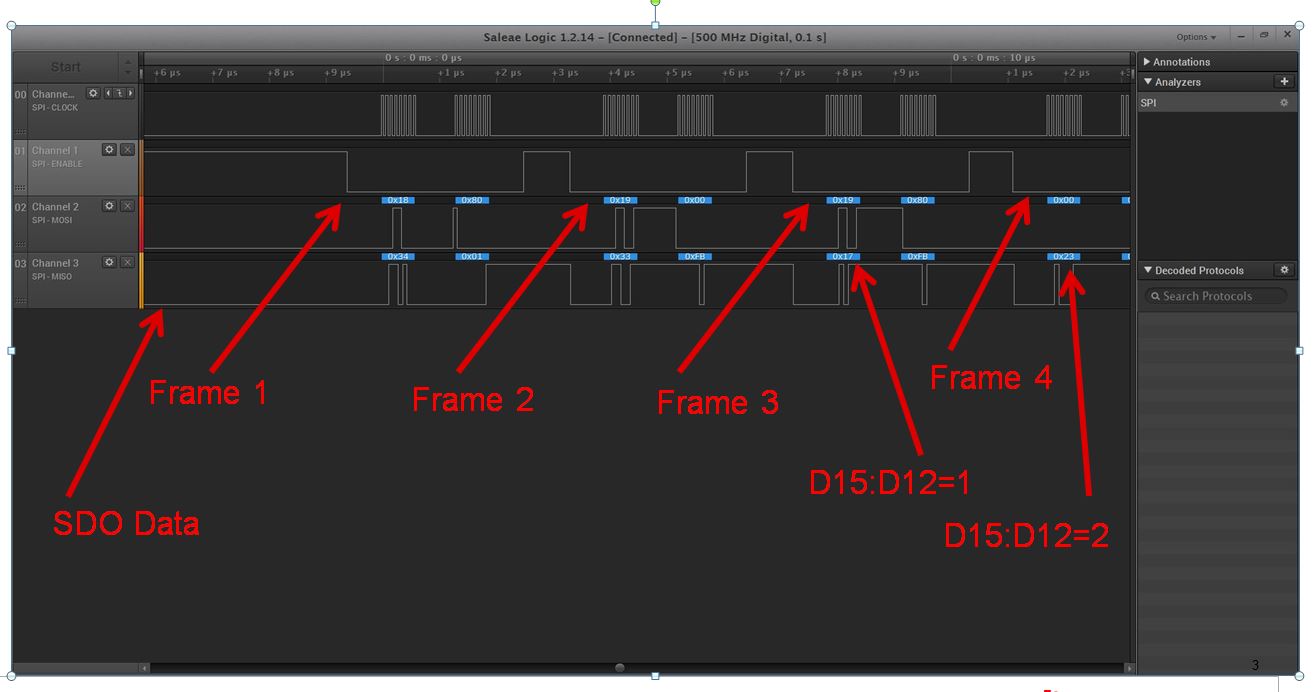
In the datasheet of ADS79xx, as shown below, what is the meaning of "analog I/P setting after chan cahnge" and "acquisition phase"?
Thanks!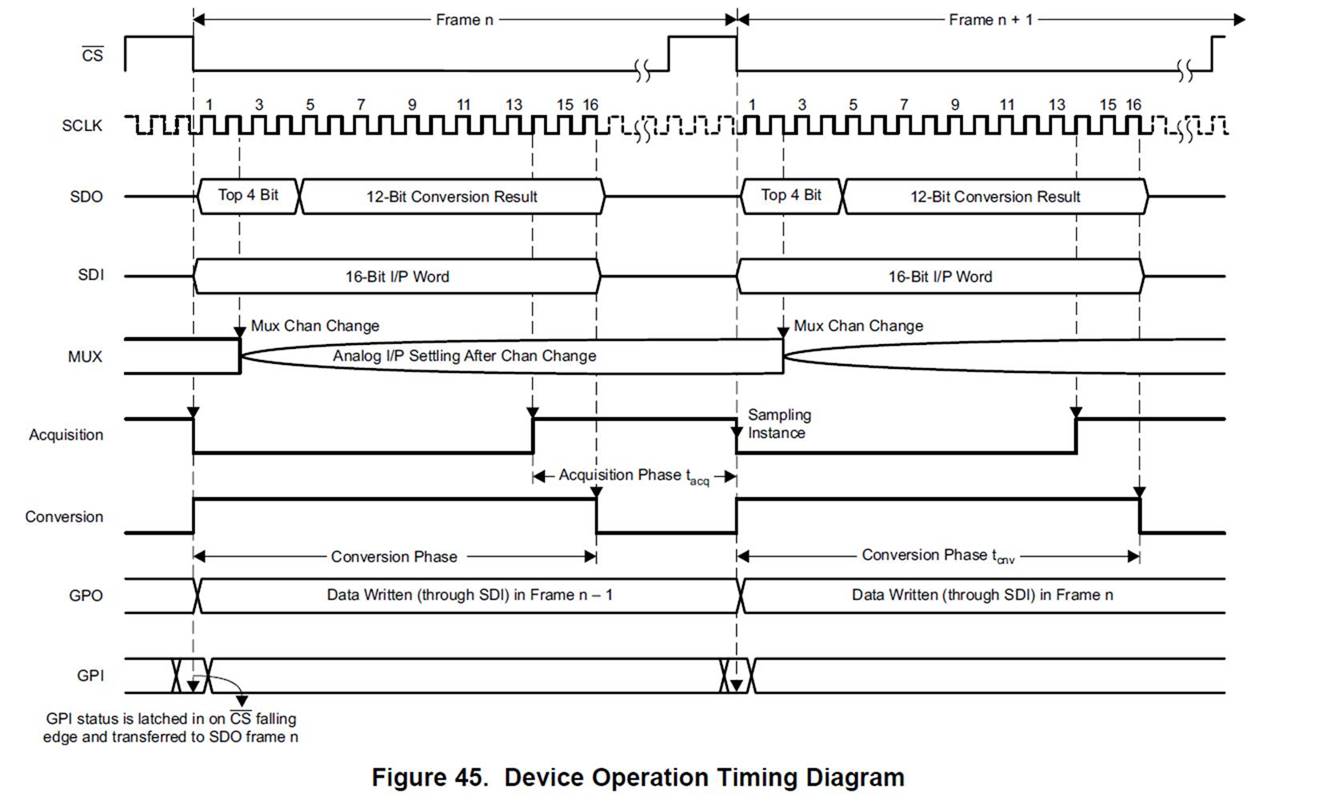
Hi team,
In the datasheet of ADS79xx, as shown below, what is the meaning of "analog I/P setting after chan cahnge" and "acquisition phase"?
Thanks!