This thread has been locked.

If you have a related question, please click the "Ask a related question" button in the top right corner. The newly created question will be automatically linked to this question.

ADS7828: Help in verificatin of schematic

Part Number: ADS7828

Hello Everyone

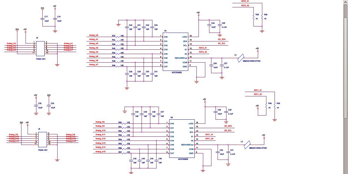
We are using ADS7828 in one of our sensing board (2 of them in a single board) as we have 16 analog channels. 

We have came up with a schemtic in which ADC0_A1 and ADC0_A0 are put in different states to provide two different 

I2C address. Before going to final routing and PCB manufacturing, i needed some help in verification of the schematic if 

there is any thing else which need to be added in order to remove the noise or this would work. 

  • Hi Shailendra

    Schematic looks ok. Please see my comments

    1. I have one comment on reference pin connection. You have used ferrite bead in series with REFIN pin. Reference pin is required to provide peak current during conversion. I would not recommend use of inductive element between VDD and REFIN connection unless your ADC sampling speed is low.

    2. SDA/SCL pins will need pull up resistor to VDD. Resistor value between 1k to 10k is typically used for pull up resistor.

    3. You can increase address pin pull-up / pull down resistor values up to 10k to save some power.

    Thanks & Regards
    Abhijeet
  • Hi 

    Thanks for confirming it. 

    1. We are not doing fast sampling. The process at othe end change very slowly. Our sampling speed is one sample per 1 minute. 

    2. SDA/SCL is already pulled up. It was a part of same schematic in different page. 

    3. As this would be running on DC power, so power consumption won't be a issue. 

    Thanks