This thread has been locked.

If you have a related question, please click the "Ask a related question" button in the top right corner. The newly created question will be automatically linked to this question.

ADS1278 Frequency modulator on the inputs

Other Parts Discussed in Thread: ADS1278, OPA1632

Hi,

I have design a board around the ADS1278. I have copied down some EVM board parts to be sure that my tracks, my plans (ground and power) and my components (capacitors, reference voltage...) are good. My configuration is "Hight precision" and my clock is 20MHz (frequency modulator at 5MHz). I use single ended inputs without differential amplifier. I have put all the AINN to VREF, but because my results was too bad, I put them now to AGND (my AINP input ranges is 2.5V now).

When I put an AINP to AGND, the AINP is clean (my noise is below 5mv, without specific frequency). The Code peak-to-peak for 20 measures has an average below 200. I have bought an EVM board to compare my results. I have modified the EVM Channel 1 to be in the same conditions : AINN to AGND and I removed the 2 resistors at the input of the amplifier (R17, R18). I added a 33k resistor in parallel of the C0G capacitor (C20) because the amplifier (U11) adds an impedance on the other channels that improve the results (i think). I put this resistor on my board too. The Code p-p for 20 mesures of AGND has an average of 100 with the EVM board.

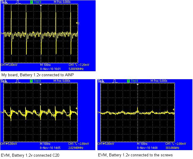
When I put a battery of 1.2V to an AIPN of my board, this AINP input gets voltage peaks of 30mv at 5MHz (frequency modulator). With the EVM board, I haven't got these peaks if i connect the battery to the screws, but i have 10mv peak to peak on AINP if I connect the battery on the C0G input capacitor (C20) (this configuration is close to my board). I have disconnected all the AINN from the ground of my board, exepted the Channel 1 (I think the modulator operates over all the channels in the same time, so a surge current is possible), but the voltage peaks persist. With the battery as input, the Code peak-to-peak of my board is 8000, the EVM Code p-p is 105 if connected to the screw, 230 if connected to C20.

There has to be an explanation of the presence of the frequency modulator peak at the AINP input... Someone has an idea ? Help is welcome !

Thanks.

PS : I join screenshots of my oscilloscope. The probe is between AGND and the positive contact of the battery (1.2V).


  • Hi Thierry, 

    The OPA1632 is on the EVM board to drive the delta sigma modulator. You are going to need something that can drive current in order to charge the modulator sampling capacitor every time that a sample is taken. On your board, you state that you remove the op amp and the problems are beginning. You are going to want to have something that can drive the modulator. You state in your system that the modulator samples every 5MHz and coincidently the "ringing" appears at the same frequency. In your first picture, you can see that there is a lot of ringing when the battery is connected directly to the ADC input without and filtering. This is a combination of the battery attempting to provide enough current to charge the modulator cap causing overshoot in combination with charge kickback from the modulator when the sample is taken. You will also notice that when C20 is included, the amplitude of the "spikes" decreases. The cap acts as both a charge reservoir for the modulator cap and in combination with the line resistance to create a RC filter cutting out some of the higher frequencies. However, you are still seeing charge kickback from the modulator sampling. What you need to do is isolate the battery from the modulator using an op amp that is fast, can supply enough current to charge the modulator cap, and settle within the time the modulator samples. 

    The reference of the ADS1278 needs to have some bulk capacitance to act as a charge reservoir for every time that the ADC takes a sample. Usually, we recommend having a 10uF to 47uF capacitor placed as close to the pin as possible. 

    Additionally, here is some reading on driving a SAR ADC. A lot of the concepts relating to the analog input hold true for a delta sigma explaining settling and charge kick. 

    Designing SAR ADC Drive Circuitry, Part I: A Detailed Look at SAR ADC Operation,” Analog Zone, 2005.
    Designing SAR ADC Drive Circuitry, Part II: Input Behavior of SAR ADCs,” Analog Zone, 2005.
    Designing SAR ADC Drive Circuitry, Part III: Designing The Optimal Input Drive Circuit For SAR ADCs,” Analog Zone, 2007.
    Regards,
    Tony Calabria 

  • Hi Tony,

    Thanks for your reply. I have found my mistake : my C0G capacitors close to the ADC were 2.2pF and not 2.2nF (mistake when I passed my order...). With 2.2nF, my signals are clean on my board. The battery was a test solution. The final application uses photodiodes with op amp, so I think additional op amp as buffers are not useful (with the prototype, the noise is about 70µV, so accurate measures is not necessary).

    I have some questions about the schematic and the layout of the EVM board, I hope you can answer these questions.

    1 - On schematic, the ADC pin number 7 is named REFENB, and is not connected. The ADS1278 Datasheet says it's a DGND pin. Why this difference ? On the EVM, this pin is connected to GND, but not track is visible (I suppose this pin is connected to the GND Plan under the ADC...). What is the good use for this pin ?

    2 - Is the EVM board made with 5 layers ? The documentation of the  EVM shows 4 layers, but I think there is a 5th layer with a ground plan. Without this 5th layer, the plane under the ADC would not be connected, and the AGND and DGND will be "virtual". I have consider ADC ground specifications found in various documentations, and I have connected my AGND with my DGND just under the ADC with a slit on a plan. Is it a good way to reduce the noise between Numeric and Analogic parts ?

    Thanks for your help.

    Regards,
    Thierry Lechevallier

  • Thierry, 

    For your first question, see here:

    http://e2e.ti.com/support/data_converters/precision_data_converters/f/73/t/72823.aspx

    The ADS1278EVM is a 4 layer board. The ground layer is shown on page 46 of the User's Guide. You will notice that the bottom right hand corner is isolated. This was to make sure any noise from the switcher network which creates the +/-10V does not interfere with the rest of the board. The six layout documents are as follows

    Top Silkscreen 

    Top Layer

    First Internal Plane (GND)

    Second Internal Layer (power)

    Bottom Layer

    Bottom Silkscreen


    Regards,

    Tony Calabria