Hi all,
I am trying to obtain 1 mV absolute accuracy over 5V full-scale range with ADS1262. This is to be achieved without any offset or gain calibration. ( Calibration is kind of hard for our production process. )
So, I post my schematics first :
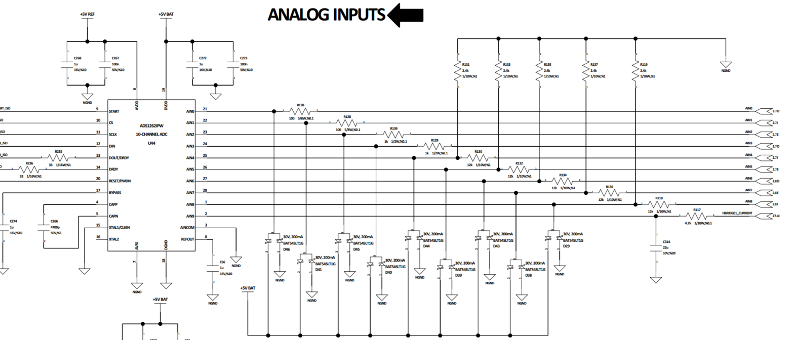
Circuit Details :
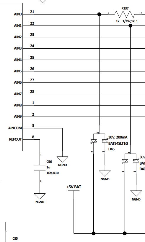
1) AIN0-AIN1 have 100 ohm ADC input resistors.
2) AIN2-AIN3 have 1kohm ADC input resistors. ( I am trying to achieve 1 mV accuracy with these two inputs )
3) AIN4-5-6-7-8 have 12k/2.4k resistive dividers to make these inputs 30V compatible.
4) AIN9 is used to monitor a current in the other part of the board.
5) All inputs except for AIN9 have Schottky protection diodes.
6) I use REF5050 5V reference voltage ( as it is better than internal reference). Reference voltage is connected to AVDD pin of ADS1262 in order not to lose any analog inputs.
7) I think layout is pretty good as well with ADC basics are all taken into consideration.
ADC Details :
1) No offset calibration or gain calibration is done.
2) Sample rate is 2400 SPS.
3) PGA is bypassed.
4) Sinc4 filter is used.
5) Chop mode off.
6) Internal Reference voltage is enabled. ( For temperature monitoring, external reference is used for ADC )
My initial reasoning:
+ Absolute input range is VAVSS-0.1 to VAVDD+0.1. So, 0V-5V full-scale range is OK.
+ Non-calibrated maximum offset voltage is 800 uV, which is 0.8mV.
+ 150 nA input current creates 0.15mV over 1kohm input resistance.
+ CMRR, PSRR and INL values are all too good be considered for 1 mV accuracy.
+ Gain error is not important because PGA is bypassed.
+ 0.8mV+0.15mv = 0.95mV. So, i guess that 1 mV absolute accuracy could be a reasonable target. I know temperature drift will affect my absolute accuracy but i am OK with 1 mV absolute accuracy at room temperature.
Test results :
A) I conducted tests with AIN2 and AIN3 over 5V FSR. Measurements are compared with calibrated Fluke multimeter. ( whose absolute accuracy is 1 mV as well )
B) At lower input voltages, an accuracy of 1 mV or better is observed. However, absolute error increases linearly towards 5V. It reaches maximum of 5mV-6mV near 5V input.
Evaluation :
1) I wanted to see if i can get better results with reduced sampling rate. I reduced sampling rate to 25 SPS and only marginal improvement was achieved.
2) REF5050 reference voltage is not 5000mv, Fluke reads it as 4999mV ( I don't know how close it is actually to 5000mV). So, this may incur some error. I am actually going for a better reference voltage IC. But i don't have the new IC yet.
3) ADS1262 Datasheet says :
"A third option for ADC reference is the internal analog power supply. However, an increase of linearity error
results with this connection, and therefore, use this option only for less-critical applications, such as ADC selfdiagnostics.
For critical applications, do not not use power-supply reference option. For applications that use the power supply voitage as the reference voltage, connect the power-supply voltage to the external reference inputs, and
select the appropriate external reference bits in the REFMUX register. "
This is exactly what i did. I connected external reference to AVDD in order not to lose any of my analog inputs. Datasheet even suggests that even if i want to use AVDD as reference, i should do this by connecting AVDD to one of reference AIN pins.
So, my first question is that could this be the reason for my very high absolute error ?
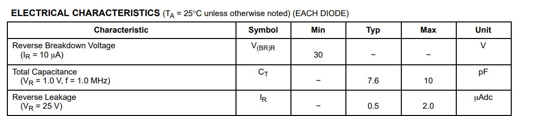
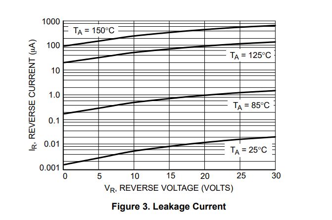
4) ADS1262 EVM has some nice C0G capacitors for input filtering. I don't have those but Schottky diodes have some capacitance and along with 1k input resistance, low-pass filter is formed with 9 MHz cut-off frequency.
My second question is that could lack of input filtering results in such a huge error ?
5) I am surprised by the linear increase of my error.
Offset error shape would be :

Gain error shape would be :
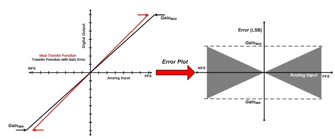
So, my error looks more like a gain error. As i turned off PGA , i would expect my absolute error to be more like a flat error of offset error. This is obviously not the case.
Again, i check the datasheet. Even though i turned off PGA, i would like to introduce gain error just like G = 1. Datasheet states that maximum uncalibrated gain error is 300 ppm.
This corresponds to G = 1,0003 for worst-case scenario. For Vin = 4900 mV, i get VADC = 4901.47 mV. 1.47 mV maximum error.
I calculated 0.95 mV from offset voltage and input current. To this, i add 1.47 mV from gain error for a worst-case absolute error of 2.42 mV.
My third question is that is gain error still valid for bypassed PGA scenarios ?
------------------------------------------------------------------------------------------------------------------------------------------------------------------------
As you can see, i am getting much more than that towards 5V FSR. I feel like i have one grave mistake that creates such a high absolute error. I would like take some advise on what i am doing wrong.
Thanks in advance for you replies.