Dears:
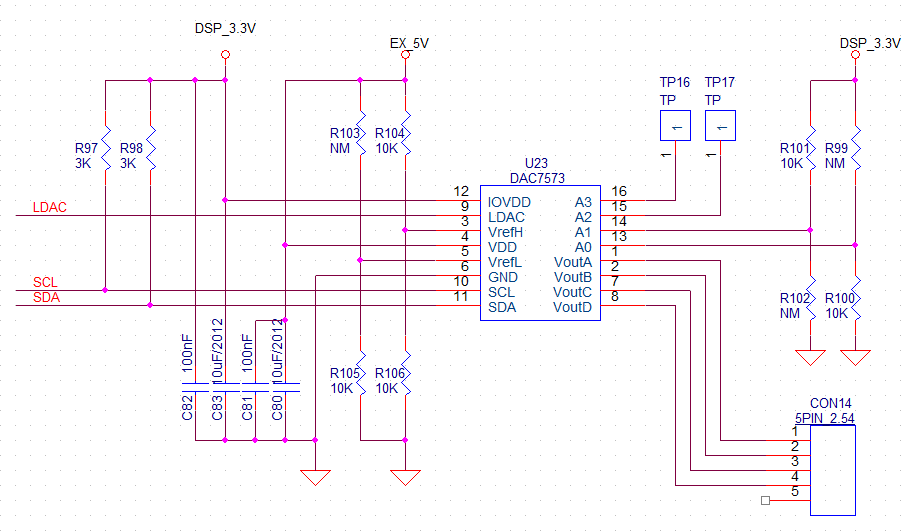
Could you kindly help to check the design:
1. Address Use A0, A1. If A2, A3 is not used, is it OK about the below design?
2. If the DAC output VREFL and VREFH circuits is together, is it wrong, how can we design it?.
3. Does the DAC output require an OP AMP configuration? If necessary, how can we design it?.


