This thread has been locked.

If you have a related question, please click the "Ask a related question" button in the top right corner. The newly created question will be automatically linked to this question.

TLV5614: LDAC* Pin's Timing Requirements/Specs are not on the Datasheet

Part Number: TLV5614
Other Parts Discussed in Thread: TMS320C203

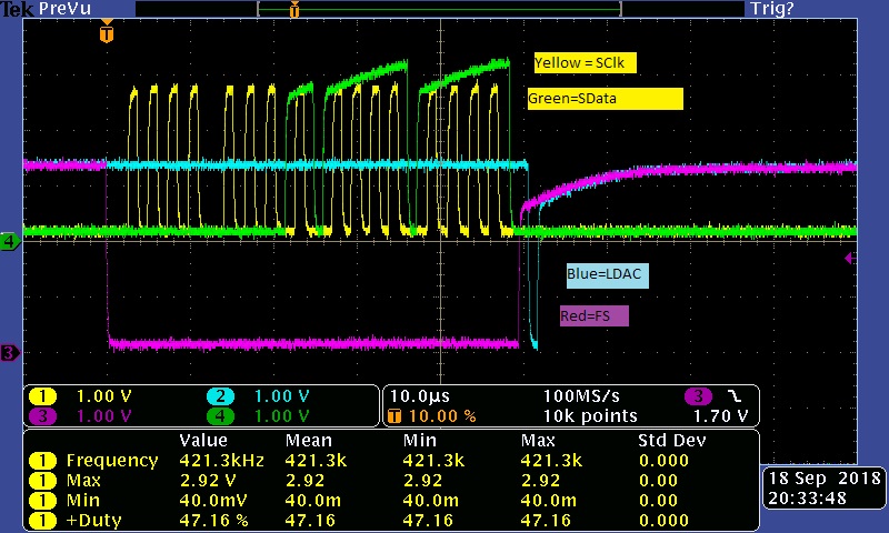
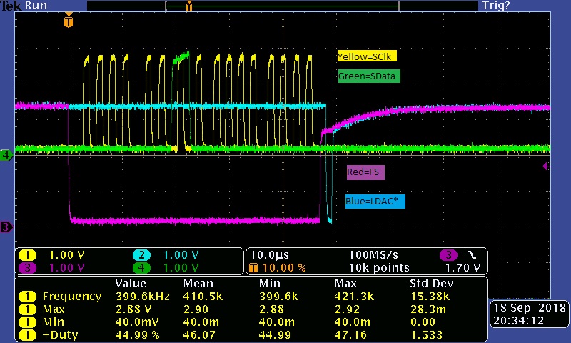
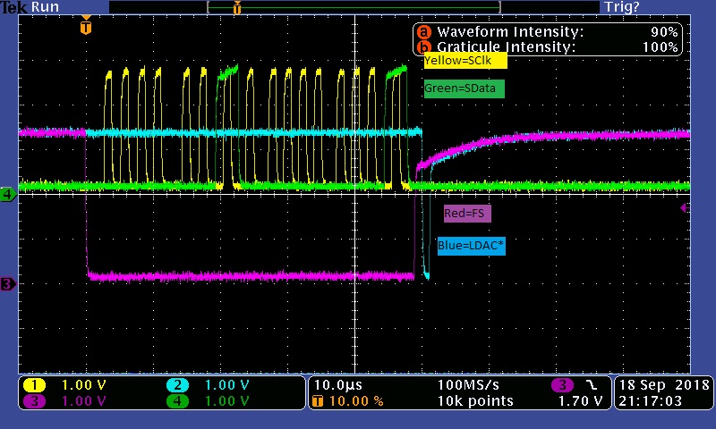
The TLV5614's rev B datasheet does nor address the LDAC* pin's timing requirements.  Can some insight be provided?

Background   I'm having issues with the output updating consistently.  Seems to update every other time.

I'm following the datasheet timing requirements to load the register, which are: 

CS* low, then FS low.  Then load 16 bits while both CS* and FS low.  Then FS hi.

After this (update of the input register), pulse LDAC* low.  The delay (after FS hi before pulsing LDAC* lo) = ~1us, and LDAC* is low for ~1us before returning LDAC* HI.

Any specs or suggestions?

  • Hi Rick,

    Thank you for your query. The TLV5614 being an old part, it somehow doesn't have the timing specs for LDAC mentioned. It doesn't have a ready EVM so I am not able to provide you a tested answer.

    I just went through the assembly code in the applications section of the datasheet and did a basic calculation. Looks like 1 us setup and hold time for LDAC should be fine. However, I am not able to conclude the state of CS during LDAC toggle from your post. I think CS should be HIGH when LDAC toggles. Please confirm. In case you are still facing the problem, please send me a scope shot of the waveforms and we will debug further.

    Regards,
    Uttam Sahu
    Applications engineer, Precision DACs
  • Hi Uttam,

    I have CS* tied to GND, as in a legacy design.  If CS* goes high, traditionally it means the IC will ignore all inputs... surprised at your suggestion.

    TLV5614 Bench Results

    The first 3 figures are scope traces, then analog values. The 0V baselines are different for 2 signals (centerline for 2, 2 div's lower for the other 2).  The clock reaches ~2.8V quickly, same as other signals.  DVdd = 3.3V

    Datasheet Vih = 2V for DVdd=2.7V

                            =2.4V for DVdd=5.5V


    Input code 0x01FF


    Input code 0x0200


    Input code 0x0201


    Various DAC0 hex input codes and DMM measurements of DAC0 Outputs.


    AVdd=5V. Vref=2.048V. Vout = 2*Vref/(input code), 1LSB=1mV.


    Notice the output moves for only every other input code, even at the low end.

  • I believe the waveforms above conform to the datasheet's Figure 1 p.7, and the Serial Interface - Three Wire on p.12.

    My take on the datasheet's TMS320C203 op code (p.19), is
    FS goes high (the commented area says they need a ClkX negative edge before FS goes high again), and
    much later (after DACs B-D inputs registers are loaded, p.20), then take CS* hi.
  • Suggest TI modify the datasheet.

    The solution I found is:  SClk must be normally high.  Scope of successful data input is below.  According to datashet p.13, clock MUST go high after FS goes HI (again no mention of LDAC). 

    Therefore, I conclude the datasheet's Figure 1 (p.7) is incomplete (no LDAC* signal); and either in error (or misleading) since SClk can NOT be "don't care" at the end of the sequence, it MUST go high.

  • I moved the SClk (yellow) last rising edge to occur before the LDAC* low pulse, and before FS rises.  Although not explicitly stated in the datasheet, it seems consistent with the example programs, specifically if updating DACs simultaneously.