This thread has been locked.

If you have a related question, please click the "Ask a related question" button in the top right corner. The newly created question will be automatically linked to this question.

ADS1292R: I can't read dataset...

Part Number: ADS1292R

Hi, I'm a korean beginner developer, so please understand that I'm not good at using Eng.

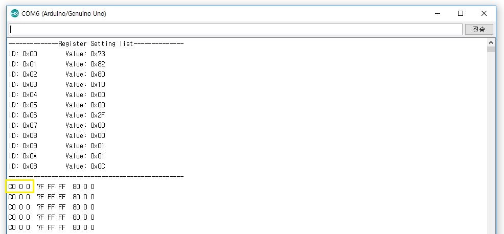
I'm developing a ECG shield for arduino Uno. I successed SPI communication between Uno-ADS1292R, but I couldn't read the correct data. I know that It occurs by hardware error, not SPI error. because I could read C00000 7FFFFF 7FFFFF< that is header of 72bit-dataset.
Finally, I found the GND misconneted with VREFP not VREFN that can make critical error.(My mistake)

So I will change my schematic and i will order PCB board within a few day. 1)Are there other problems? Please fix my schematic if it has some error.


And also, I'll try to read data with externer RLDREF not interner VREF, before PCB is delivered. But I'm confused how to setting register.

2) I wonder that RLDREF is related with VREF because I want to read data without VREF and can't use VREF at all as I said above.


3) If it isn't, How can I set the register?

  • Hello Seonjo,

    Thanks for your post!

    I have reviewed your schematic and have a few comments.

    For AVDD and DVDD, I recommend adding a 1uF and 0.1uF to both with respect to ground.
    Connect IN2N, IN2P, RESPMODN, and RESPMODP to AVDD.
    What input filter do you have on IN1N and IN1P?
    When START is tied low, the OPCODE must be used. If this is intentional, leaving START tied low is fine.
    Add a 10k series resistor to your GPIO pins before terminating to GND.
    I'm not sure why you have the resistors tied on your digital pins DRDY, DOUT, DIN, SCLK, CS. Can you provide a little information about what you're trying to do with these?

    Take a look at the schematic from the post below for guidance on analog input filters and digital pin connections.

    e2e.ti.com/.../1615410

    You will need VREF in order to read data. For the time being so you can continue testing, I would recommend scraping the trace from the capacitors C8 & C9 to VREFP and VREFN, then soldering in two fly wires in order to connect the capacitors correctly. This should allow you to continue testing.
  • Thanks for your advicee. I'll modify my circuit by referring to your advice.

    Uno has 5V logic level and the chip has 3.3V logic level, so I tried to shift the level by Valtage Division Rule with 1.8k : 3.3k ohms.

    But It was bad idea. I knew there were open-collector(drain) effect after PCB order , so I changed the part with Level shifter that your company provide. The schematic is a old thing.

    In channel 1 case. there were connected with serially HP and LP-RC filter(5~2000Hz) and parallely circuit protection structure
  • I'll add power separation(Lineal power regulator) and CH2 after success to read data... because I should learn more about that. Then, can I try with this one?

  • Hello Seonjo,

    Now that the changes have been made your schematic looks good!

    May I ask why you chose to filter out 1-4Hz on the inputs?
  • I'm developing it for education, that my class-mate can understand and compare data before and after filtering