


I have a follow on question to this thread:
Peter Gatchell's (https://e2e.ti.com/members/365439) response dated Mar 31, 2015 9:47 PM provides a clear explanation of the input voltages.
My issue comes when I view Table 18 in the ADC08D1520 data sheet:
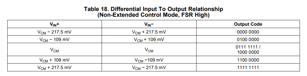
The table header clearly states that this table is describing the condition where the FSR bit is high. Per the previous discussion and the value for Vin on page 14, the peak-to-peak voltage is 870mV when FSR is high. However, the table shows a peak-to-peak of 435mV (exactly half the 870mV).
Is this table correct? If it is correct, is there explanation for the difference?
Thanks,
Eric


