This thread has been locked.

If you have a related question, please click the "Ask a related question" button in the top right corner. The newly created question will be automatically linked to this question.

ADS4149: Questions regarding ADS5474 and interleaving

Part Number: ADS4149
Other Parts Discussed in Thread: ADS54J40, ADS54J40EVM, ADS54J60, ADS41B49, , LMK04821, LMK04208, LMK04828

Dear Specialists,

My customer is considering a system of 14 to 16 bits and 1Gsps.

I would be grateful if you could advise.

---

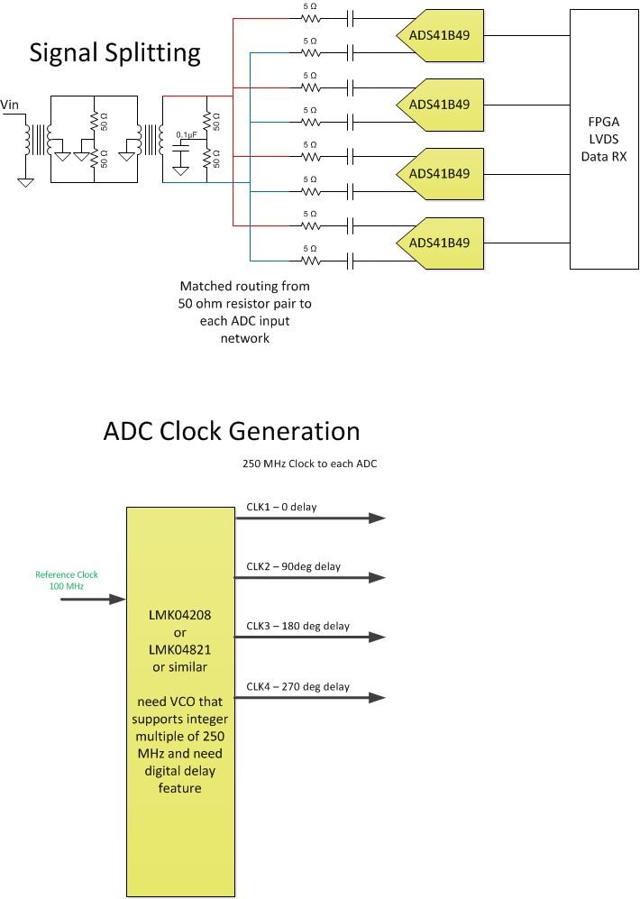
There is a demand for realization with a parallel ADC because there is a limitation in the production of the substrate.

I'd like to use Interleave like SLAU247, are there any reference designs that match the above conditions?

To realize 1 Gsps, I think that four 250 Msps devices will be used.

I would like you to propose it together with the A / D converter.

---

I appreciate your great help in advance.

Best regards,

Shinichi

  • Hi Shinichi
    I would like to get a little more information to help provide the best answer.
    What is the maximum signal frequency that the customer needs to digitize?
    Is the DC information in the signal important, or can the signal to converter path be AC-coupled? If AC-coupling is acceptable what is the minimum frequency needed?
    Best regards,
    Jim B
  • Hi Jim,

    Thank you for your reply.

    I confirmed the customer.

    Could you please see below.

    ---

    (1) The maximum frequency is 235MHz.
    I'd like to sample 1Gsps.

    (2)I'd like to use AC coupling, the minimun frequency is 100kHz.
    The system lowest frequency is 400kHz.

    ---
    I'm looking forward to waiting your recommended design.

    I appreciate your great help.

    Best regards,
    Shinichi
  • Hi Shinichi
    The customer could implement a solution using 4x 14-bit 250MSPS ADC converters with LVDS interfaces (CMOS interfaces are not recommended at 250 MSPS). It will take a lot of FPGA I/O to receive the data signals from all converters but can be done. The clocking solution will need to generate 4 synchronized ADC clocks that are offset in timing to achieve combined sample rate of 1 GSPS.
    With this solution the customer will need to develop or buy technology to compensate for the spurs created by offset, gain and sampling timing mismatch between the 4 interleaved converters.
    A much easier approach would be to use something like the ADS54J60 or ADS54J40 ADC which is a dual 16 or 14 bit ADC sampling at 1GSPS. In this case the I/O is high speed serial JESD204B with much fewer pairs of data running at a higher data rate. Since the clock is embedded within each serial stream the board layout is usually easier with this technology. In this approach the customer does not have to compensate for interleaving spurs. The ADS54J40 product folder and ADS54J40EVM tool folder have links to the datasheet, user guide and hardware design files.
    Is there any way they can use the second approach? I think it will be easier to achieve compared with the challenges of interleaving correction.
    I hope this is helpful.
    Best regards,
    Jim B
  • Hi Jim,

    Thank you for your reply.

    Currently, the customer is highly interested in 4ADC solution.

    There are some problems he should be solved, but he tries.

    JESD204B is simple solution, but his company couldn't adopt this.

    He mentioned JESD204B has very high datarate(Gbps order), their using PWB maker can't produce.

    I keep introducing the products with JESD204B, but this time the customer is going to prototype with 4ADC solution.

    Could you please provide reference circuit of 4ADC with around circuit.

    I appreciate your great help and cooperation.

    Best regards,
    Shinichi
  • Hi Shinichi
    Understood. I'm working on a block diagram illustrating the main features they need to include in the design.
    Does the customer have any specific FPGA brand or part number they are targeting for this design?
    Best regards,
    Jim B
  • Hi Shinichi

    Here is my suggested configuration for the customer. I highly recommend using ADS41B49 (buffered inputs) instead of the ADS4149 (unbuffered inputs). The unbuffered inputs of the ADS4149 will inject sampling noise back to the driving circuitry. If 4 ADCs are trying to sample the same input signal the interaction of this sampling noise will significantly degrade performance. 

    I hope this is helpful.

    Best regards,

    Jim B

  • Hi Jim,

    Thank you for your reply.

    I'll share your suggestion with the customer.

    If he has an additional question, I consult you again.

    Also, he is thinking to use Xillinx FPGA, but he hadn't decided part number yet.

    I appreciate your great help and continuous support.

    Best regards,
    Shinichi
  • Hi Jim,

    I sent your suggestion to the customer and he has two questions.

    I would be grateful if you could advise.

    ---
    1. How can LMK04208 and LMK04821 generate a phase difference of 90 to 270 deg at 250 MHz promptly?

    These devices has many delay function, I'm not sure which register should use.

    Could you please advise how accurately can 90deg phase shift be realized?

    2. About spurious
    As you mentioned before "In this solution, four interleaved
    We need to develop a technique to compensate for the spurs caused by the mismatch between offset, gain, and sampling timing between the converters. "

    In case
    As for the offset / gain, an adjustment method plan appears, but as for the sampling timing, I can only think about how to reduce the spurious by randomizing the input of each ADC.
    However, since this method also needs to switch at high speed, it is unclear whether there is a corresponding device, so I'm not sure whether it can be used.

    It will be appreciated if you can give us a bit more advice on this part.

    I appreciate your great help.

    Best regards,
    Shinichi
  • Hi Shinichi

    Regarding point 1.
    For the LMK04208 or LMK04828, the VCO would be configured to operate at 3000 MHz. (30x the input reference frequency of 100 MHz)
    To generate 250 MHz for each ADC the output dividers will be set to 12. The digital delay function allows the outputs to be delayed in half or full steps of the VCO period, so the different ADC clock outputs could be delayed by the following number of steps using this method:
    ADC 1 - no delay
    ADC 2 - 3 VCO periods
    ADC 3 - 6 VCO periods (or inverted polarity with no delay)
    ADC 4 - 9 VCO periods (or inverted polarity with 3 VCO period delay)

    For point 2.
    To optimize the interleave timing, additional delay fine-tuning could be done using the 25 ps analog delay steps in the LMK04208 device. To do the tuning an input test signal must be applied, and then the ADC timing will be adjusted to minimize the timing related interleave spurs or fine-tune the measured phase offset between the digitized signals.
    Randomizing can theoretically be used, but as you say this would not be easy to implement in a board level solution.

    I hope this is helpful.

    Best regards,
    Jim B
  • Hi Jim,

    Thank you for your reply.

    I understand the customer's requirement is realized by combination of digital delay and analog delay.

    I'll share this suggestion with the customer.

    I appreciate your great help.

    Best regards,

    Shinichi 

  • Hi Jim,

    The customer keeps condidering about interleaving sampling and has a request.

    I would be grateful if you could advise.

    ---

    Do you have a control IP for interleave.

    I found one IP provided by SP devices, it also include delay control, it is useful.

    But it only provide for teledyne.

    I couldn't find another supplier.

    If you know another supplier, could you please inform, or you have original program, could you please provide?

    It takes many time to develop control interleaving ADC program, I'd like to save the time by using a completed IP.

    ---

    I appreciate your great help.

    Best regards,

    Shinichi

  • Hi Shinichi

    TI does not have any interleaving IP to optimize the sample timing, gain, or offset of the multiple converters.

    The easiest approach is with the aid of a known test signal that can be applied to all 4 converters.

    The basic calibration process will proceed similar to the following steps:

    1. With test signal off, adjust offset of each ADC to match the ADC output codes for all 4 converters.
    2. With test signal on, adjust gain of each ADC to match the ADC min/max output codes for all 4 converters.
    3. With test signal off, re-adjust offset of each ADC to match the ADC output codes for all 4 converters.
    4. With test signal on, re-adjust gain of each ADC to match the ADC min/max output codes for all 4 converters.
    5. With test signal on, fine-tune sampling timing to minimize spurs at Fs/2-Fin, Fs/4+Fin and Fs/4-Fin

    Best regards,

    Jim B

  • Hi Jim,

    Thank you for your reply and suggestion.

    If you know the supplier except SP device, could you please let me know.

    I appreciate your great help.

    Best regards,

    Shinichi

  • Hi Shinichi
    I'm not aware of any vendors other than SP device that provide this type of IP for system level use.
    Best regards,
    Jim B
  • Hi Jim,

    Thank you for your reply.

    I understand that there are no vendors that can satisfy customers' demands except SP device.

    I'll share with the customer.

    Best regards,

    Shinichi