This thread has been locked.

If you have a related question, please click the "Ask a related question" button in the top right corner. The newly created question will be automatically linked to this question.

ADS1120: Configuration registers being set only sometimes

Part Number: ADS1120

I have an application in which the ADS1120 is being used in the following manner. A piezoresistive bridge is excited by the 0.5mA IDAC source and read differentially between AIN0 and AIN1. Two trimmer pots are read on AIN2 and AIN3.

The SPI lines are being driven by a STM32L011.

I have an issue setting the configuration registers. No matter what I write to the registers, the readback values are 0xFF or 0x00.

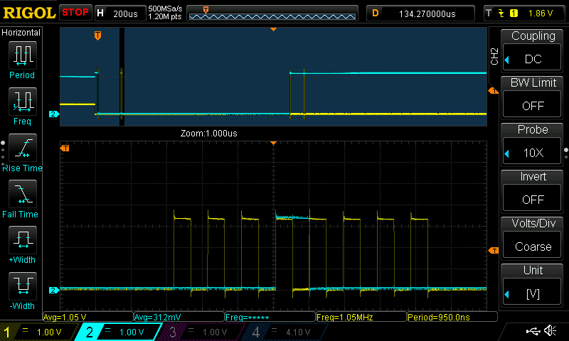
Furthermore, if I attempt to issue a RDATA command as shown by the following capture of MOSI and SCK

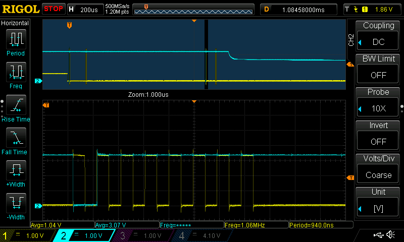
the next two bytes that I read are always 0x7F, 0xFF like in the following capture of MISO and SCK

I can see that the SPI line transitions on MOSI, MISO and SCK are sharp without much overshoot or undershoot. Furthermore, the ADS1120 seems to be clocking out something, since the first byte is always 0x7F.

I have verified that are no dips or brownouts on either AVDD or DVDD pins and GND connections of both pins have less than 0.1 Ohm impedance to the ground plane.

I have racked my brains trying to think of a reason why this could be happening, since the chip worked perfectly in my last iteration of the design. All that's changed between the iterations is that the four 47 Ohm resistors are moved to the bottom plane with vias to the top plane on either side adjacent to the corresponding pins on the microcontroller and ADS1120.

I would be very grateful for any advice anyone could offer me.

Thanks in advance,

Gaurav.

  • Hi Gaurav,

    Welcome to our e2e forum! Your screen captures did not seem to come through properly. Can you send them again?
  • I have updated the post with working links to screenshots. Sorry for the confusion.
  • Hi Gaurav,

    There are several things that are unclear, mostly the WREG and RREG commands. Make sure that the CS has a good connection and remains low throughout the entire communication transaction. It appears you have a 4-channel scope, can you send shots of the WREG and RREG commands and data with SCLK, MISO, MOSI and CS on the same scope plot (to be clear I mean WREG on one plot and RREG on another plot)?

    Can you send me the configuration register settings you think you are writing to the ADS1120? Also, are the RREG and WREG commands written to individual registers (one at a time) or as a block of registers? Please send the values you are writing to the device.

    Before issuing RDATA, have you sent the START/SYNC command and then waited for the conversion to complete?

    What path are you using for sensor excitation? Is the current coming from REFP0? If so, have you measured the output voltage? And have you made sure there is a complete path to ground? What reference are you using? If you are attempting to use the REF0 as a ratiometric measurement then REFN0 must go to GND. Also remember that there is an IDAC compliance voltage, so the voltage drop from the IDAC output through the sensor to ground must be less than the compliance voltage (AVDD-0.9V) as the current source cannot drive all the way to the supply rail and provide a constant current at the selected setting.

    Best regards,
    Bob B
  • Hi Bob,

    I apologize for being incomplete in my reporting of the details.

    Following is the configuration procedure pseudocode

    1. Drive CS low
    2. Delay 1 ms
    3. Write 1 byte - 0x06 (Reset)
    4. Delay 1ms
    5. Write 5 bytes -
      1. 0x43 - WREG 4 bytes starting from register 0
      2. 0x0a - AIN0 and AIN1 differential input - Gain 32 - PGA enabled
      3. 0x04 - Continuous conversion mode
      4. 0x05 - IDAC 500 uA
      5. 0xc0 - IDAC1 routed to REFN0
    6. Delay 1 ms
    7. Write 1 byte - 0x23 (Read 4 bytes starting from register 0)
    8. Delay 1 ms
    9. Read 4 bytes
    10. Delay 1 ms
    11. Write 1 byte - 0x08 (Start)
    12. Delay 1 ms
    13. Drive CS high

    Following is the pseudocode for my loop

    1. Drive CS low
    2. Delay 1 ms
    3. Write 1 byte - 0x10 (RDATA)
    4. Delay 1 ms
    5. Read 2 bytes
    6. Delay 1 ms
    7. Drive CS high

    I have checked that CS has a good connection and remains low throughout the transaction. While I have a 4 channel scope, I sadly neglected to add testpoints on the PCB and can hold probes on only two pins at a time reliably. However, I have sequentially probed two at a time CS and SCK, SCK and MISO, SCK and MOSI and all transitions look clean and sharp with no ringing.

    I can try to solder thin wires to the pins and setup my probes to capture all 4 channels simultaneously if you think it would help in troubleshooting on Monday morning when I head to work.

    Following is the way the piezoresistive sensor is connected.

                            REFN0 (IDAC1 500 uA)
                                 |
                               /   \
                           R       R
                          /            \
             AIN0 --                 -- AIN1
                          \            /
                           R       R
                               \   /
                                 |
                              GND

    Bridge input resistance is 5-6 KOhm and AVDD is 5V, so 2.5-3 V drop over the bridge is well within the 4.1V limit. For the same sensor used with the last board revision, I have also tested it with my Fluke calibrator and the IDAC functions within expected accuracy.
    Full span output of the bridge is ~30mV.

    The problem here is that the register readback gives 0xff on all 4 bytes and used to return expected values on my last board revision. This current non-working revision has only two changes

    1. IDAC1 output used to be AIN3, now it is REFN0
    2. 4x47 Ohm resisters used to be on same side as microcontroller and ADS1120, now they are on the bottom side.

    Best regards,
    Gaurav 

  • Hi Gaurav,

    It does not appear that there is anything incorrect in your procedure that would cause an issue. I would suggest that you toggle CS between WREG and RREG commands.

    If the registers were written correctly, then you should see continuous conversions if you probe the DRDY pin every 50ms. You should also see a voltage drop from REFN0 to ground.

    When you issue the RDATA command, make sure that you have allowed enough time for the conversion to be completed before attempting the read the result.

    Best regards,
    Bob B
  • Dear Bob,

    You are correct when you say that if the registers were written correctly, then you should see continuous conversions every 50ms. I have verified that on my previous working board revision.
    In this case, it is absolutely evident that the IC is not responding to SPI communications for the setting of registers.

    As for not waiting after issuing RDATA, I am fine with having slightly stale conversion results as stated in the datasheet page 37.


    Is the correct functioning of this IC highly layout dependent? Would it help with troubleshooting if I shared signal layers screenshots of working last revision and non-working current revision?

    Alternately, is this IC highly susceptible to damage in manual hand-assembly with either an incorrect heating profile or ESD safety?
    My last working revision was all assembled in a reflow oven after automated pick and place while this non-working revision was manually placed and soldered with hot-air rework tools.

    These two points are the only reasons I can speculate as to why the IC does not work despite having good power connections and clean SPI transitions on SCK, CS and MOSI pins.

    Regards,
    Gaurav.

  • Hi Gaurav,

    There is always the possibility of the device being damaged during a hand build, but I don't think this is the problem. You can check if the device is operating correctly by powering up the device while monitoring DRDY. The ADS1120 in normal startup (or power up) mode will take one conversion and go to a low power state. When conversion completes, DRDY will go from a high state to a low state. Verify that this action is taking place prior to attempting to send any commands.

    While reviewing the scope shots again I see that there appears to be a 'float' condition on the SCLK line shortly before the SCLKs are issued. Is this the powering up of the micro? It is possible that you are having a timing issue when you first power up. Before attempting to communicate to the ADS1120 make sure that both AVDD and DVDD are fully powered and at the nominal voltage and then wait about 1ms before sending a RESET command. Also frame each communication with CS. If there is a timing issue with the commands, this toggling of CS will reset the ADS1120 SPI communication in case either the device is not ready to communicate or there was an error in the previous communication.

    Best regards,
    Bob B