This thread has been locked.

If you have a related question, please click the "Ask a related question" button in the top right corner. The newly created question will be automatically linked to this question.

Programming ADS1298 with MSP430F1611

Other Parts Discussed in Thread: MSP430F1611, ADS1298

4426.ada1298_msp430f1611.rarTo whom it may concern,

                                     I am trying to program ads1298 with MSP430F1611, but there are some problems as follows.

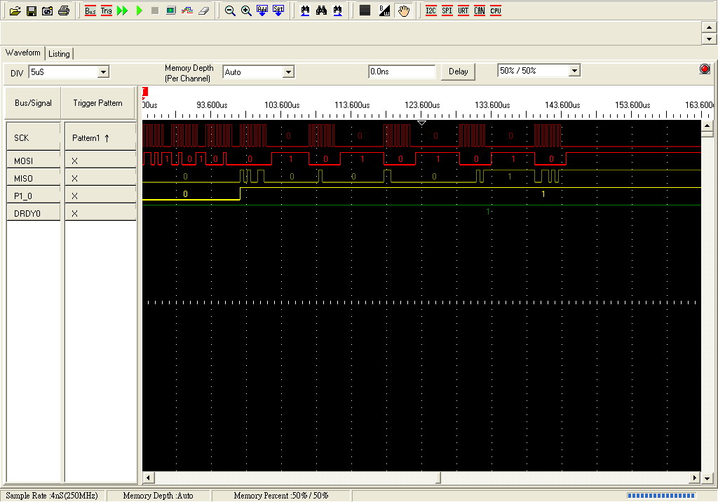
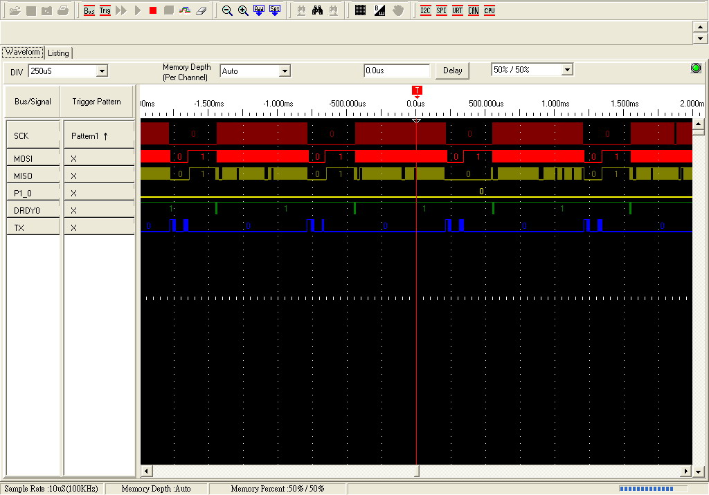
1. I must repeat the RREG command to get the correct value of the register.

for example, I WREG the registers first, and then PREG the registers, the code as follow.

  while (!(IFG1 & UTXIFG0));           
  TXBUF0 = 0x41;
 
  while (!(IFG1 & UTXIFG0));
  TXBUF0 = 0x04;
 
  while (!(IFG1 & UTXIFG0));            // WREG CONFIG1 0xA6
  TXBUF0 = 0xA6;
 
  while (!(IFG1 & UTXIFG0));            // WREG CONFIG2 0x10
  TXBUF0 = 0x10;
 
  while (!(IFG1 & UTXIFG0));            // WREG CONFIG3 0xC0
  TXBUF0 = 0xC0;
 
  while (!(IFG1 & UTXIFG0));            // WREG 0x04    0x05
  TXBUF0 = 0x05;
 
  while (!(IFG1 & UTXIFG0));            // WREG 0x05    0x06
  TXBUF0 = 0x06;
 

  while (!(IFG1 & UTXIFG0));           
  TXBUF0 = (0x45);
  
  while (!(IFG1 & UTXIFG0));
  TXBUF0 = 0x07;

  for (i = 0; i < 8; i++)               // WREG CHnSET 0x05
  { 
   while (!(IFG1 & UTXIFG0));
   TXBUF0 = 0x05;
  }
 
  for (i = 0; i < 2; i++)
  {
  while (!(IFG1 & UTXIFG0));            // RREG CONFIG3
  TXBUF0 = 0x21;
 
  while (!(IFG1 & UTXIFG0));
  TXBUF0 = 0x01;
  }
 
  while (!(IFG1 & URXIFG0));
  RES[0] = RXBUF0;
 
  while (!(IFG1 & URXIFG0));
  RES[1] = RXBUF0;
  
  for (i = 0; i < 2; i++)
  {
  while (!(IFG1 & UTXIFG0));            // RREG CONFIG3
  TXBUF0 = 0x23;
 
  while (!(IFG1 & UTXIFG0));
  TXBUF0 = 0x01;
  }
  
  while (!(IFG1 & URXIFG0));
  RES[2] = RXBUF0;
 
  while (!(IFG1 & URXIFG0));
  RES[3] = RXBUF0;

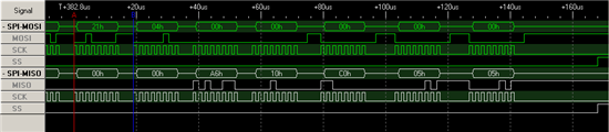
It seems something strange when I PREG the registers.


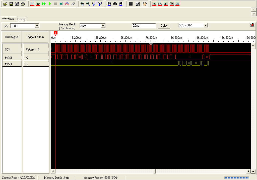
2. I could not get the values of the eight channels when I set START pin to 1 and  use the  RDATAC command.

My whole code is attached


  • Hi Sheng-Fu,

    I'll look into this for you, but its going to take me a day or two.  How exactly do you call you SPI setup routine?  The function is there, but I don't see you calling it from within your main() program.

  • Hi Tom,

    I'm sorry for missing some code. Please look at the attached files included the code , the circuit and the pin signal output. I use the internal clock in ads1298 and set the CLK pin output. When I set START=1 or set START pin High, I pick up the DRDY signal as the attached file. It seems abnormal. Please give me some suggestions. Thanks.

    Sheng-Fu

    2376.ads1298_msp430f1611_1.rar

  • Sheng-Fu,

    You need to remember that the transfer takes place only if the master sends clocks.  After your RREG command, you can supply 'dummy' data to initiate the SPI clock - Modify the read portion of your code as follows and let me know what you see:

      while (!(IFG1 & UTXIFG0));            // RREG starting at address 1
      TXBUF0 = 0x21;
      while (!(IFG1 & UTXIFG0));            // 5 Registers
      TXBUF0 = 0x04;

      while (!(IFG1 & UTXIFG0));
      TXBUF0 = 0x00;
      while (!(IFG1 & URXIFG0));
      RES[0] = RXBUF0;

      while (!(IFG1 & UTXIFG0));
      TXBUF0 = 0x00;
      while (!(IFG1 & URXIFG0));
      RES[1] = RXBUF0;

      while (!(IFG1 & UTXIFG0));
      TXBUF0 = 0x00;
      while (!(IFG1 & URXIFG0));
      RES[2] = RXBUF0;

      while (!(IFG1 & UTXIFG0));
      TXBUF0 = 0x00;
      while (!(IFG1 & URXIFG0));
      RES[3] = RXBUF0; 

      while (!(IFG1 & UTXIFG0));
      TXBUF0 = 0x00;
      while (!(IFG1 & URXIFG0));
      RES[4] = RXBUF0;

  • Hi Tom,

                You are great. Thank you, but I still meet some trouble. When I revise the code that you provided, the results in RES are shifted to the wrong positions as bellow.

    So I try to add another 'dummy' data, the code as follow, then I get the correct results.

      while (!(IFG1 & UTXIFG0));            // RREG starting at address 1
      TXBUF0 = 0x21;
      while (!(IFG1 & UTXIFG0));            // 5 Registers
      TXBUF0 = 0x04;

      while (!(IFG1 & UTXIFG0));
      TXBUF0 = 0x00;
      
      while (!(IFG1 & UTXIFG0));            // another dummy data
      TXBUF0 = 0x00;
     
      while (!(IFG1 & URXIFG0));
      RES[0] = RXBUF0;

    ...........
     

    I use a logic analyzer to find the timing sequence, the results are the same, except the MOSI sequence. The upper is for your code, the lower is for my revised code.


    Best regards

    Sheng-Fu

  • Sheng-Fu,

    Please keep in mind the SPI interface of the MSP430 - for each transmit there is a receive, in both your sequence and mine, the SDO from the ADS1298 is coming out with the first 'dummy' transfer, yet it shows up in the processor (RES[0]) only after transfer +1.  I don't recall the specifics of the receive buffer on the MSP430F1611, but I suspect if you clear the receive buffer or review the way you are clearing the flags on both the transmit/receive side of things you can remove that 'extra' cycle.  

  • Hi Tom,

               You are right. I try to find any thing about the receive buffer or the flag of the control register from the USER GUIDE, the key point may be the OE bit in the UxRCTL. So, when I supply the 'dummy' data, I will check the OE bit in the UxRCTL. If the OE bit is true, it may indicate the previous data in the receive buffer was not read yet, then I read the previous data from  the receive buffer first and toggle P1.0 state. The partial code and the timing sequence are as follow. Look at the timing sequence, the P1.0 state is changed one time, and then is not changed, it shows the OE bit is fault when the previous data is not read.

      while (!(IFG1 & UTXIFG0));            // RREG starting at address 1
      TXBUF0 = 0x21;
     
      while (!(IFG1 & UTXIFG0));            // 5 Registers
      TXBUF0 = 0x04;
       
      while (!(IFG1 & UTXIFG0));
      TXBUF0 = 0x00;
     
      if(U0RCTL & OE)
      {
       P1OUT ^=0x01;
       while (!(IFG1 & URXIFG0));
       STAT[0] = RXBUF0;
      }
     
      while (!(IFG1 & URXIFG0));
      RES[0] = RXBUF0;
     
      while (!(IFG1 & UTXIFG0));
      TXBUF0 = 0x00;
     
      if(U0RCTL & OE)
      {
       P1OUT ^=0x01;
       while (!(IFG1 & URXIFG0));
       STAT[1] = RXBUF0;
      }
     
      while (!(IFG1 & URXIFG0));
      RES[1] = RXBUF0;
     
      while (!(IFG1 & UTXIFG0));
      TXBUF0 = 0x00;
     
      if(U0RCTL & 0xOE)
      {
       P1OUT ^=0x01;
       while (!(IFG1 & URXIFG0));
       STAT[2] = RXBUF0;
      }
     
      while (!(IFG1 & URXIFG0));
      RES[2] = RXBUF0;
     
      while (!(IFG1 & UTXIFG0));
      TXBUF0 = 0x00;
     
      if(U0RCTL & 0xOE)
      {
       P1OUT ^=0x01;
       while (!(IFG1 & URXIFG0));
       STAT[3] = RXBUF0;
      }
     
      while (!(IFG1 & URXIFG0));
      RES[3] = RXBUF0; 
     
      while (!(IFG1 & UTXIFG0));
      TXBUF0 = 0x00;
     
      if(U0RCTL & 0xOE)
      {
       P1OUT ^=0x01;
       while (!(IFG1 & URXIFG0));
       STAT[4] = RXBUF0;
      }
     
      while (!(IFG1 & URXIFG0));
      RES[4] = RXBUF0;
    }


    Best regards,

    Sheng-Fu


  • Hi Tom,

                 I just finish the 16-channel data acquistion with two ads1298 and send only one channel data to PC by RS-232 with sampling rate 1K Hz. My test signal is Vpp 100mV, 1Hz sine wave generated from a signal generator. When I reconstruct the test signal by LabVIEW, the waveform is not good. Why?

    My code is 4212.ada1298_6.rar

  • Hi Sheng-Fu,

    Not sure how much I can help you here.  The interface from your MSP430 to the PC may be the issue.  Try simply putting in a static DC level to the ADS1298 and verify you have the correct output codes.  That should take the ADS1298 and a portion of your SPI program out of the equation.  From there you will need to look and see if you are properly concatenating the data (three bytes of data) and transferring it to Lab View properly.