Hi,
Our customers are using two ADS1255 to develop analytical instruments.
Xtal is used for the main ADC and CLKOUT output is connected from the main ADC to the sub ADC.
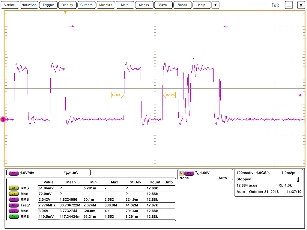
However, when the clock output is turned on, the Xtal oscillation and the two ADC conversion results are abnormal.
Variation at input short circuit: 0.001 V -> 0.1 V
I think PCB layout may be a problem. The device used is as follows.
Xtal: CX5032GA08000HOHEQ Kyocera
C: 15 pF

There is questions.
It can be understood that the conversion result of the sub ADC gets worse due to this influence. Why is the conversion result of the main ADC also abnormal?
Customers say Xtal's oscillation will be abnormal. Is this incorrect?
Does the two ADCs share CLKOUT as a clock?
If so, you can understand that the conversion results of the two ADCs are abnormal.
Please tell me the cause and measures.
Best regards,
Hiroshi