This thread has been locked.

If you have a related question, please click the "Ask a related question" button in the top right corner. The newly created question will be automatically linked to this question.

ADS7253: SPI interface Question

Part Number: ADS7253

Hi TI Team

I am using ADS7253IRTER chip for measuring the analog voltage. I want to use internal reference voltage for the ADC. Could you please tell me the steps for configuring the CFR, REFDAC_A, and REFDAC_B registers and readback those registers. Please do tell me the steps for reading the Conversion Data. 

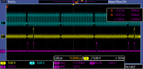
I am using Microsemi-SmartFusion2 FPGA (M2S005-VF400I) and this ADC is connected to FPGA Fabric. I want to develop custom SPI interface code in VHDL/verilog for the configuration and Reading the Conversion Data.

I am getting confused with the Timing diagram provided in the datasheet. Could you please suggest the procedure for configuring the ADC and Reading the conversion Data.

Configuration:

--> Interface Mode : 32-CLK, dual-SDO mode

--> Output data format : Straight binary format

--> ADC reference voltage source : Use internal reference


Below are my values to be written  in the registers.

CFR Write value = 0x8040

REFDAC_A Write Value = 0x9FF8 (VRef = 2.5V)

REFDAC_A Write Value = 0xAFF8 (VRef = 2.5V)

CFR Read Control Word = 0x3000

REFDAC_A Read Control Word = 0x1000

REFDAC_A Read Control Word = 0x2000

Conversion Data Read Control Word = 0x8040

Please correct me if my control word is wrong as per above configuration requirement.

  • Hi Chandan,

    The register details for the ADS7523 you described look fine to me. One thing to keep in mind is that you need 48 SCLK cycles to write or read the various registers. When you are simply running conversions, you only need 32 SCLK cycles (see Figure 90).
  • Hi sir

    Could you please provide me the steps for configuring the ADC.

    Could you please provide any reference code of the implementation of SPI interface for this part, this will be a great help for me for implementing in vhdl.

    If you provide timing diarsm that would be also fine.

  • Hi Chandan,

    I don't have a code example to send you at the moment, but maybe this will help you understand the interface a little better. Referring to Figure 1, Table 4 and Figure 90, to write to the CFR you would start by setting /CS low and then start shifting in your 0x8040 command. For reading and writing the registers, the command transmit length has to be 48 clocks long with the configuration command/data loaded into the 16 MSB's.
    So, to write the CFR with your desired configuration, you'd need to send 0x804000000000 with data valid on the falling SCLK edge and then bring /CS back high. You would do the same thing for writing to the DAC registers (0x9FF800000000 and 0xAFF800000000). To read from the CFG register, just modify the command to be 0x3000000000. The desired register contents will be output on the 16 MSB's of the next frame.

  • Hi sir

    As per your suggestion, I have written the data in below sequence:

    Write CFR Register = 0x804000000000, 48 CLK Pulses are generated, then

    write 0x000000000000, 48 CLK Pulses are generated, then

    ReadBack CFR Register = 0x300000000000,  48 CLK Pulses are generated, then I am generating 48 clock pulses, that i am able to Read 0x004000000000. Is the Reading is correct? . As per Datasheet, I should Read 0x304000000000. Please correct me if I am wrong. But when I am checking in oscilloscope, i am missing the MSB Bit.

    In the same fashion I have written REFDAC_A and REFDAC_B Registers with 0x9FF800000000 and 0xAFF800000000 respectively. When I am reading these registers i am getting 0x9FF8 and 0xAFF8 respectively.

    But when I am checking in oscilloscope, i am missing the MSB Bit. is the read data is correct of REFDAC_A and REFDAC_B?

    Please Suggest how to read the conversion data and what should be the control word to be written to read the digital data.

  • Can you send along a scope capture showing the details?
  • Hi sir

    Please find the below scope of the data which is being written and Read to/from CFR, REFDAC_A and REFDAC_B Registers.

    1) CFR Write/Read. In the scope, Blue Color represents SPI_CLK, Pink color represents DIN to ADC and Yellow color represents SDO_DOUTA. CFR Write Value = 0x8040 and CFR Read Value = 0x3000


    2) REFDAC_A Write/Read. In the scope, Blue Color represents SPI_CLK, Pink color represents DIN to ADC and Yellow color represents SDO_DOUTA. REFDAC_A Write Value = 0x9FF8 and REFDAC_A Read Value = 0x1000

    3) REFDAC_B Write/Read. In the scope, Blue Color represents SPI_CLK, Pink color represents DIN to ADC and Yellow color represents SDO_DOUTA. REFDAC_A Write Value = 0xAFF8 and REFDAC_A Read Value = 0x2000

    Please suggest how to read the ADC conversion Data. what control word we need to send and how many clock pulses are required if i am operating in 32-clk, dual SDO Mode.

  • Hi Chandan,

    Thank you for the screen shots! Clearly SDO is valid on the rising SCLK edge, so perhaps I need to revise my drawings. Can you modify SDI so that it is valid on a rising SCLK edge as well (shift DIN left by 1/2 clock) and re-run your tests?
  • Hi Chandan,

    Have you made any progress?
  • Dear Sir

    Thank you for your support. Now i am able to Read the ADC Conversion Data.